


Peripheral Control Block
4-1
CHAPTER
4
PERIPHERAL CONTROL BLOCK
4.1 OVERVIEW
The Am186ER and Am188ER microcontroller integrated peripherals are controlled by
16-bit read/write registers. The peripheral registers are contained within an internal
256-byte control block—the peripheral control block (PCB). Registers are physically located
in the peripheral devices they control, but they are addressed as a single 256-byte block.
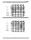
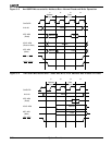
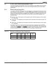
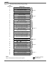
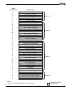
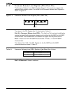
Figure 4-1 shows a map of the peripheral control block registers.
Code that is intended to execute on the Am188ER microcontroller should perform all writes
to the PCB registers as byte writes. These writes will transfer 16 bits of data to the PCB
register even if an 8-bit register is named in the instruction. For example, out dx, al
results in the value of ax being written to the port address in dx. Reads to the PCB should be
done as word reads. Code written in this manner will run correctly on the Am188ER
microcontroller and on the Am186ER microcontroller. Unaligned reads and writes to the PCB
result in unpredictable behavior on both the Am186ER and Am188ER microcontrollers.
The peripheral control block can be mapped into either memory or I/O space. The base
address of the control block must be on an even 256-byte boundary (i.e., the lower eight
bits of the base address are 00h). Internal logic recognizes control block addresses and
responds to bus cycles. During bus cycles to internal registers, the bus controller signals
the operation externally (i.e., the RD
, WR, status, address, and data lines are driven as in
a normal bus cycle), but the data bus, SRDY, and ARDY are ignored.
At reset, the Peripheral Control Block Relocation Register is set to 20FFh, which maps the
control block to start at FF00h in I/O space. An offset map of the 256-byte peripheral control
register block is shown in Figure 4-1. See section 4.1.1 on page 4-4 for a complete
description of the Peripheral Control Block Relocation (RELREG) Register.