


System Overview
3-14
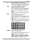
If CLKSEL1 is held Low during power-on reset, the chip enters the
Divide by Two clocking mode where the fundamental clock is derived
by dividing the external clock input by two. If Divide by Two mode is
selected, the PLL is disabled. See Table 3-4, “Clocking Modes,” on page
3-16.
This pin is latched within three crystal clock cycles after the rising edge
of RES
. Note that clock selection must be stable four clock cycles prior
to exiting reset (i.e., RES
going High).
If S6/CLKSEL
1 is to be used as a programmable interrupt (PIO29) in
input mode, the input device must not drive the pin Low during power-
on reset. S6/CLKSEL
1 defaults to a PIO input with pullup, so it does
not need to be driven High externally.
SCLK Serial Clock (output, synchronous, three-state)
This pin supplies the synchronous serial interface (SSI) clock to a slave
device, allowing transmit and receive operations to be synchronized
between the microcontroller and the slave. SCLK is derived from the
microcontroller internal clock and then divided by 2, 4, 8, or 16,
depending on register settings.
An access to any of the SSR or SSD registers activates SCLK for eight
SCLK cycles (see Figure 12-5 and Figure 12-6 on page 12-8). When
SCLK is inactive, it is held High by the microcontroller. SCLK is three-
stated during ONCE mode.
SDATA Serial Data (input/output, synchronous)
This pin transmits and receives synchronous serial interface (SSI) data
to and from a slave device. When SDATA is inactive, a weak keeper
holds the last value of SDATA on the pin.
SDEN1–SDEN0 Serial Data Enables (output, synchronous)
These pins enable data transfers on ports 1 and 0 of the synchronous
serial interface (SSI). The microcontroller asserts either SDEN1 or
SDEN0 at the beginning of a transfer and deasserts it after the transfer
is complete. When SDEN1–SDEN0 are inactive, they are held Low by
the microcontroller. SDEN1–SDEN0 are three-stated during ONCE
mode.
SRDY Synchronous Ready (input, synchronous, level-sensitive)
This pin indicates to the microcontroller that the addressed memory
space or I/O device will complete a data transfer. The SRDY pin accepts
an active High input synchronized to CLKOUTA.
Using SRDY instead of ARDY allows a relaxed system timing because
of the elimination of the one-half clock period required to internally
synchronize ARDY. To always assert the ready condition to the
microcontroller, tie SRDY High. If the system does not use SRDY, tie
the pin Low to yield control to ARDY.
TMRIN0 Timer Input 0 (input, synchronous, edge-sensitive)
This pin supplies a clock or control signal to the internal microcontroller
timer 0. After internally synchronizing a Low-to-High transition on
TMRIN0, the microcontroller increments the timer. TMRIN0 must be
tied High if not being used.