


Chip Select Unit
5-6
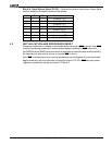
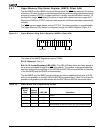
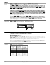
5.5.2 Low Memory Chip Select Register (LMCS, Offset A2h)
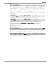
The Am186ER and Am188ER microcontrollers provide the LCS chip select pin for the
bottom of memory. Because the interrupt vector table is located at 00000h at the bottom
of memory, the LCS
pin has been provided to facilitate this usage. The LCS pin is not active
on reset, but any write access to the LMCS Register activates this pin.
The Low Memory Chip Select is configured through the LMCS Register (see Figure 5-2).
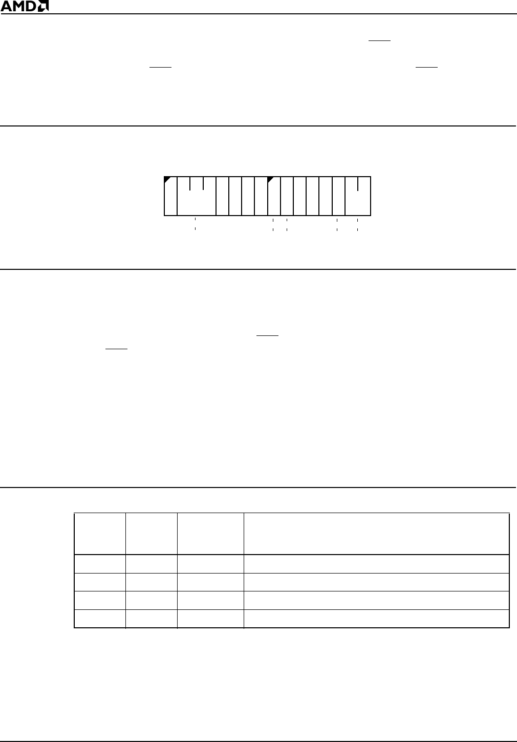
Figure 5-2 Low Memory Chip Select Register (LMCS, offset A2h)
The value of the LMCS Register at reset is undefined.
Bit 15: Reserved—Set to 0.
Bits 14–12: Upper Boundary (UB2–UB0)—The UB2–UB0 bits define the upper boundary
of the memory accessed through the LCS
chip select. Because of the timing requirements
of the LCS
output and the nonmultiplexed address bus, the number of programmable
memory sizes for the LMCS Register is reduced compared to the 80C186 and 80C188
microcontrollers. Consequently, the number of programmable bits has been reduced from
eight bits in the 80C186 and 80C188 microcontrollers to three bits in the Am186ER and
Am188ER microcontrollers.
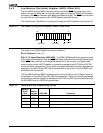
The Am186ER and Am188ER microcontrollers have a block size of 512 Kbyte, which is
not available on the 80C186 and 80C188 microcontrollers. Table 5-3 outlines the possible
configurations and the differences between the 80C186 and 80C188 microcontrollers and
the Am186ER and Am188ER microcontrollers.
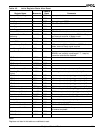
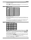
Table 5-3 LMCS Block Size Programming Values
Memory
Block
Size
Ending
Address UB2–UB0 Comments
64K 0FFFFh 000b
128K 1FFFFh 001b
256K 3FFFFh 011b
512K 7FFFFh 111b
Not available on the 80C186 and 80C188 microcontrollers
1
15
70
0
UB2–UB0
11 1
PSE
11 1
A19
R1–R0
R2
DA