


C-13
REGISTERS
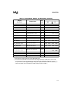
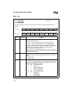
CCR1
CCR1
no direct access
†
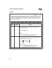
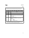
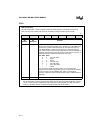
The chip configuration 1 (CCR1) register enables the watchdog timer and selects the bus timing
mode. Two of its bits combine with three bits of CCR0 to control wait states and bus width.
7 0
1 1 0 1 WDE BW1 IRC2 0
Bit
Number
Bit
Mnemonic
Function
7:6 1 To guarantee proper operation, write ones to these bits.
5 0 To guarantee proper operation, write zero to this bit.
4 1 To guarantee proper operation, write one to this bit.
3 WDE Watchdog Timer Enable
Selects whether the watchdog timer is always enabled or enabled the
first time it is cleared.
0 = always enabled
1 = enabled first time it is cleared
2 BW1 Buswidth Control
This bit, along with the BW0 bit (CCR0.1), selects the bus width.
BW1 BW0
0 0 illegal
0 1 16-bit only
1 0 8-bit only
1 1 BUSWIDTH pin controlled
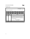
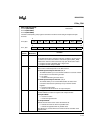
†
The CCRs are loaded with the contents of the chip configuration bytes (CCBs) after reset, unless
the microcontroller is entering programming modes (see “Entering Programming Modes” on page
16-13), in which case the programming chip configuration bytes (PCCBs) are used. The CCBs
reside in nonvolatile memory at addresses 2018H (CCB0) and 201AH (CCB1).