8XC196MC, MD, MH USER’S MANUAL
B-20
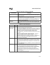
PROG# I Programming Start
During programming, a falling edge latches data on the PBUS and begins
programming, while a rising edge ends programming. The current location is
programmed with the same data as long as PROG# remains asserted, so the
data on the PBUS must remain stable while PROG# is active.
During a word dump, a falling edge causes the contents of an OTPROM
location to be output on the PBUS, while a rising edge ends the data transfer.
On the 8XC196MC and MD, PROG# is multiplexed with P2.2 and EPA2. On the
8XC196MH, PROG# is multiplexed with P2.2 and EPA1.
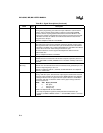
PVER
O Program Verification
During slave or auto programming, PVER is updated after each programming
pulse. A high output signal indicates successful programming of a location,
while a low signal indicates a detected error.
PVER is multiplexed with P2.0 and EPA0.
PWM1:0 O Pulse Width Modulator Outputs
These are PWM output pins with high-current drive capability.
PWM1:0 are multiplexed with P6.7:6.
RD# O Read
Read-signal output to external memory. RD# is asserted only during external
memory reads.
RD# is multiplexed with P5.3.
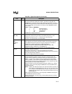
READY I Ready Input
This active high input along with the chip configuration registers determine the
number of wait states inserted into the bus cycle. The chip configuration
registers selects the maximum number of wait states (0, 1, 2, 3, or infinite) that
can be inserted into the bus cycle. While READY is low, wait states are inserted
into the bus cycle until the programmed number of wait states is reached. If
READY is pulled high before the programmed number of wait states is reached,
no additional wait states will be inserted into the bus cycle.
READY is multiplexed with P5.6.
RESET# I/O Reset
A level-sensitive reset input to and open-drain system reset output from the
microcontroller. Either a falling edge on RESET# or an internal reset turns on a
pull-down transistor connected to the RESET# pin for 16 state times. In the
powerdown and idle modes, asserting RESET# causes the chip to reset and
return to normal operating mode. The 8XC196MH provides the option of
preventing an internal reset from generating a reset on the external pin (see
“Resetting the Device” on page 13-8). After a device reset, the first instruction
fetch is from FF2080H.
RXD1:0
(MH only)
I/O Receive Serial Data 0 and 1
In modes 1, 2, and 3, RXD0 and 1 receive serial port input data. In mode 0, they
function as either inputs or open-drain outputs for data.
RXD0 is multiplexed with P1.1 and RXD1 is multiplexed with P1.3.
Table B-6. Signal Descriptions (Continued)
Name Type Description


