12-3
ANALOG-TO-DIGITAL (A/D) CONVERTER
12.3 A/D CONVERTER OPERATION
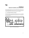
An A/D conversion converts an analog input voltage to a digital value, stores the result in the
AD_RESULT register, and sets the A/D interrupt pending bit. An 8-bit conversion provides
20 mV resolution, while a 10-bit conversion provides 5 mV resolution. An 8-bit conversion takes
less time than a 10-bit conversion because it has two fewer bits to resolve and the comparator re-
quires less settling time for 20 mV resolution than for 5 mV resolution.
You can convert either the voltage on an analog input channel or a test voltage. Converting the
test inputs allows you to calculate the zero-offset error, and the zero-offset adjustment allows you
to compensate for it. This feature can reduce or eliminate off-chip compensation hardware. Typ-
ically, you would convert the test voltages and adjust for the zero-offset error before performing
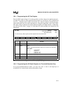
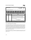
conversions on an input channel. The AD_TEST register allows you to program a zero-offset ad-
justment.
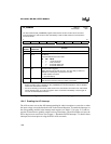
A threshold-detection compares an input voltage to a programmed reference voltage and sets the
A/D interrupt pending bit when the input voltage crosses over or under the reference voltage.
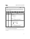
A conversion can be started by a write to the AD_COMMAND register or it can be initiated by
the EPA, which can provide equally spaced samples or synchronization with external events.
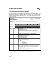
(See“Programming the EPA and Timer/Counters” on page 11-15.) The A/D scan mode of the pe-
ripheral transaction server (PTS) allows you to perform multiple conversions and store their re-
sults. (See “A/D Scan Mode” on page 5-32.)
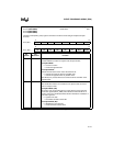
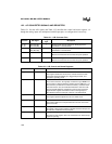
P0_PIN 1FA8H (MC, MD)
1FDAH (MH)
Port 0 Pin State
Read P0_PIN to determine the current values of the port 0 pins.
Reading the port induces noise into the A/D converter, decreasing
the accuracy of any conversion in progress. We strongly
recommend that you not read the port while an A/D conversion is in
progress. To reduce noise, the P0_PIN register is clocked only
when the port is read.
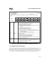
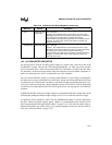
P1_PIN (MC,MD) 1FA9H (MC, MD) Port 1 Pin State
Read P1_PIN to determine the current values of the port 1 pins.
Reading the port induces noise into the A/D converter, decreasing
the accuracy of any conversion in progress. We strongly
recommend that you not read the port while an A/D conversion is in
progress. To reduce noise, the P1_PIN register is clocked only
when the port is read.
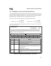
Table 12-2. A/D Control and Status Registers (Continued)
Mnemonic Address Description


