


10-3
PULSE-WIDTH MODULATOR
10.3 PWM OPERATION
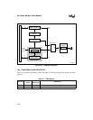
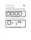
The period register (PWM_PERIOD) controls the output frequency of both PWM outputs. Each
control register (PWMx_CONTROL) controls the duty cycle (the pulsewidth stated as a percent-
age of the period) of the corresponding PWM output. Each control register contains an 8-bit value
that is loaded into a buffer when the 8-bit counter rolls over from 00H to FFH. The comparators
compare the contents of the buffers to the counter value. Since the value written to the control
register is buffered, you can write a new 8-bit value to PWMx_CONTROL at any time. However,
the comparators do not recognize the new value until the counter has expired the remainder of
the current 8-bit count. The new value is used during the next PWM output period.
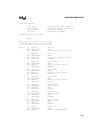
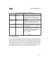
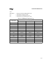
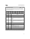
Table 10-2. PWM Control and Status Registers
Mnemonic Address Description
PWM0_CONTROL
PWM1_CONTROL
1FB0H
1FB2H
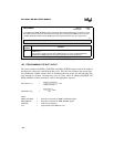
PWM Duty Cycle
This register controls the PWM duty cycle. A zero loaded
into this register will cause the PWM to output a low
continuously (0% duty cycle). An FFH in this register will
cause the PWM to have its maximum duty cycle (99.6%
duty cycle).
PWM_PERIOD 1FB4H PWM Period
This register holds a programmed value that determines
the output period of the PWM outputs. The value is
reloaded into the counter each time the count resets to
FFH.
PWM_COUNT 1FB6H PWM Counter
This read-only register contains the current value of the
decremented counter.
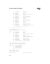
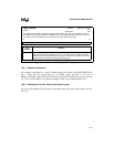
WG_OUTPUT 1FC0H Waveform Generator Output
Bits 11 and 12 (PE6 and PE7) determine whether the
corresponding pin functions as a standard I/O port pin or
as a PWM output. Bits 6 and 7 (P6 and P7) define the pin
output when the port pin function is selected.
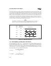
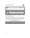
PE
x
P
x
Pin Output
000
011
1 X PWM Output