15-3
INTERFACING WITH EXTERNAL MEMORY
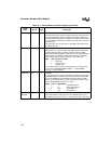
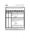
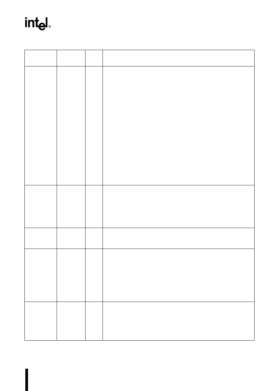
EA# — I External Access
This input determines whether memory accesses to special-purpose
and program memory partitions are directed to internal or external
memory. (See Table 4-1 on page 4-2 for address ranges of special-
purpose and program memory partitions.) These accesses are
directed to internal memory if EA# is held high and to external
memory if EA# is held low. For an access to any other memory
location, the value of EA# is irrelevant.
EA# also controls entry into the programming modes. If EA# is at V
PP
voltage (typically +12.5 V) on the rising edge of RESET#, the micro-
controller enters a programming mode.
NOTE: Systems with EA# tied inactive have idle time between
external bus cycles. When the address/data bus is idle, you
can use ports 3 and 4 for I/O. Systems with EA# tied active
cannot use ports 3 and 4 as standard I/O; when EA# is
active, these ports will function only as the address/data bus.
EA# is sampled and latched only on the rising edge of RESET#.
Changing the level of EA# after reset has no effect.
Always connect EA# to V
SS
when using a microcontroller that has no
internal nonvolatile memory.
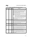
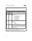
INST P5.1 O Instruction Fetch
This active-high output signal is valid only during external memory bus
cycles. When high, INST indicates that an instruction is being fetched
from external memory. The signal remains high during the entire bus
cycle of an external instruction fetch. INST is low for data accesses,
including interrupt vector fetches and chip configuration byte reads.
INST is low during internal memory fetches.
RD# P5.3 O Read
Read-signal output to external memory. RD# is asserted only during
external memory reads.
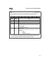
READY P5.6 I Ready Input
This active high input along with the chip configuration registers
determine the number of wait states inserted into the bus cycle. The
chip configuration registers selects the maximum number of wait
states (0, 1, 2, 3, or infinite) that can be inserted into the bus cycle.
While READY is low, wait states are inserted into the bus cycle until
the programmed number of wait states is reached. If READY is pulled
high before the programmed number of wait states is reached, no
additional wait states will be inserted into the bus cycle.
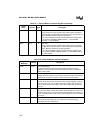
WR# P5.2 O Write
†
This active-low output indicates that an external write is occurring.
This signal is asserted only during external memory writes.
†
The chip configuration register 0 (CCR0) determines whether this
pin functions as WR# or WRL#. CCR0.2 = 1 selects WR#; CCR0.2 =
0 selects WRL#.
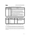
Table 15-1. External Memory Interface Signals (Continued)
Signal
Name
Port Pin Type Description


