8XC196MC, MD, MH USER’S MANUAL
15-2
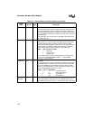
ALE P5.0 O Address Latch Enable
This active-high output signal is asserted only during external memory
cycles. ALE signals the start of an external bus cycle and indicates
that valid address information is available on the system address/data
bus. ALE differs from ADV# in that it does not remain active during the
entire bus cycle.
An external latch can use this signal to demultiplex the address from
the address/data bus.
BHE# P5.5 O Byte High Enable
†
During 16-bit bus cycles, this active-low output signal is asserted for
word and high-byte reads and writes to external memory. BHE#
indicates that valid data is being transferred over the upper half of the
system data bus. Use BHE#, in conjunction with AD0, to determine
which memory byte is being transferred over the system bus:
BHE# AD0 Byte(s) Accessed
0 0 both bytes
0 1 high byte only
1 0 low byte only
†
The chip configuration register 0 (CCR0) determines whether this
pin functions as BHE# or WRH#. CCR0.2 = 1 selects BHE#;
CCR0.2 = 0 selects WRH#.
BUSWIDTH P5.7 I Bus Width
Two chip configuration register bits, CCR0.1 and CCR1.2, along with
the BUSWIDTH pin, control the data bus width. When both CCR bits
are set, the BUSWIDTH signal selects the external data bus width.
When only one CCR bit is set, the bus width is fixed at either 16 or 8
bits, and the BUSWIDTH signal has no effect.
CCR0.1 CCR1.2 BUSWIDTH
0 1 X fixed 8-bit data bus
1 0 X fixed 16-bit data bus
1 1 high 16-bit data bus
1 1 low 8-bit data bus
CLKOUT
(MC, MD)
— O Clock Output
Output of the internal clock generator. The CLKOUT frequency is ½
the oscillator input frequency (F
XTAL1
). CLKOUT has a 50% duty cycle.
Table 15-1. External Memory Interface Signals (Continued)
Signal
Name
Port Pin Type Description


