


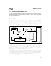

7-3
SERIAL I/O (SIO) PORT
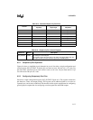
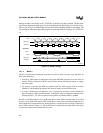
INT_PEND1 0012H Interrupt Pending 1
When set, the TI
x
bit indicates a pending transmit interrupt.
When set, the RI
x
bit indicates a pending receive interrupt.
When set, the SPE bit indicates a pending serial port receive error
interrupt. You must read the PI_PEND register to determine which
channel generated the interrupt.
P1_DIR 1F9BH Port 1 Direction
This register selects the direction of each port 1pin. Set P1_DIR.1
and P1_DIR.3 to configure RXD0 (P1.1) and RXD1 (P1.3) as high-
impedance inputs/open-drain outputs, and clear P1_DIR.0 and
P1_DIR.2 to configure TXD0 (P1.0) and TXD1 (P1.2) as comple-
mentary outputs.
P1_MODE 1F99H Port 1 Mode
This register selects either the general-purpose input/output function
or the peripheral function for each pin of port 1. Set P1_MODE.3:0
to configure TXD0 (P1.0), TXD1 (P1.2), RXD0 (P1.1), and RXD1
(P1.3) for the SIO port.
P1_PIN 1F9FH Port 1 Pin State
Four bits of this register contain the values of the TXD0 (P1.0),
RXD0 (P1.1), TXD1 (P1.2), and RXD1 (P1.3) pins. Read P1_PIN to
determine the current value of the TXD
x
and RXD
x
pins.
P1_REG 1F9DH Port 1 Output Data
This register holds data to be driven out on the pins of port 1. Set
P1_REG.1 and P1_REG.3 for the RXD
x
pins. Set P1_REG.0 and
P1_REG.2 for the TXD
x
pins.
P2_DIR 1FD2H Port 2 Direction
This register selects the direction of each port 2 pin. To use BCLK
x
as the baud-rate generator clock source for modes 0–3, or to use
mode 4 (in which case SCLK
x
# is the shift clock), set P2_DIR.1 and
P2_DIR.7 to configure SCLK0#/BCLK0 (P2.1) and SCLK1#/BCLK1
(P2.7) as high-impedance inputs/open-drain outputs.
P2_MODE 1FD0H Port 2 Mode
This register selects either the general-purpose input/output function
or the peripheral function for each pin of port 2. Set P2_MODE.1
and P2_MODE.7 to configure SCLK0#/BCLK0 (P2.1) and
SCLK1#/BCLK1 (P2.7) for the SIO port.
P2_PIN 1FD6H Port 2 Pin State
Two bits of this register contain the values of the SCLK0#/BCLK0
(P2.1) and SCLK1#/BCLK1 (P2.7) pins. Read P2_PIN to determine
the current value of the pins.
P2_REG 1FD4H Port 2 Output Data
This register holds data to be driven out on the pins of port 2. Set
P2_REG.1 and P2_REG.7 for the SCLK0#/BCLK0 (P2.1) and
SCLK1#/BCLK1 (P2.7) pins.
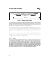
Table 7-2. Serial Port Control and Status Registers (Continued)
Mnemonic Address Description