


8XC196MC, MD, MH USER’S MANUAL
C-12
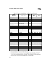
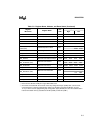
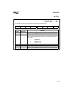
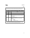
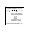
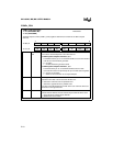
CCR0
3 ALE Address Valid Strobe and Write Strobe
These bits define which bus-control signals will be generated during
external read and write cycles.
ALE WR
0 0 address valid with write strobe mode
(ADV#, RD#, WRL#, WRH#)
0 1 address valid strobe mode
(ADV#, RD#, WR#, BHE#)
1 0 write strobe mode
(ALE, RD#, WRL#, WRH#)
1 1 standard bus-control mode
(ALE, RD#, WR#, BHE#)
2WR
1 BW0 Buswidth Control
This bit, along with the BW1 bit (CCR1.2), selects the bus width.
BW1 BW0
00illegal
0 1 16-bit only
1 0 8-bit only
1 1 BUSWIDTH pin controlled
0 PD Powerdown Enable
Controls whether the IDLPD #2 instruction causes the microcontroller to
enter powerdown mode. If your design uses powerdown mode, set this
bit when you program the CCBs. If it does not, clearing this bit when you
program the CCBs will prevent accidental entry into powerdown mode.
0 = disable powerdown mode
1 = enable powerdown mode
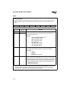
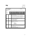
CCR0 (Continued)
no direct access†
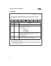
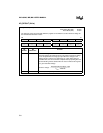
The chip configuration 0 (CCR0) register controls powerdown mode, bus-control signals, and internal
memory protection. Three of its bits combine with two bits of CCR1 to control wait states and bus
width.
7 0
LOC1 LOC0 IRC1 IRC0 ALE WR BW0 PD
Bit
Number
Bit
Mnemonic
Function
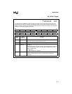
†
The CCRs are loaded with the contents of the chip configuration bytes (CCBs) after reset, unless the
microcontroller is entering programming modes (see “Entering Programming Modes” on page 16-13),
in which case the programming chip configuration bytes (PCCBs) are used. The CCBs reside in
nonvolatile memory at addresses 2018H (CCB0) and 201AH (CCB1).