


8XC196MC, MD, MH USER’S MANUAL
15-10
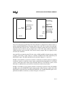
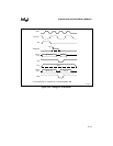
15.3 BUS WIDTH AND MULTIPLEXING
The external bus can operate as either a 16-bit multiplexed address/data bus or as a multiplexed
16-bit address/8-bit data bus (Figure 15-3).
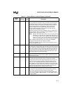
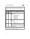
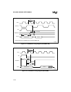
1 IRC2 Ready Control
This bit, along with IRC0 (CCR0.4), IRC1 (CCR0.5), and the READY pin
determine the number of wait states that can be inserted into the bus
cycle. While READY is held low, wait states are inserted into the bus
cycle until the programmed number of wait states is reached. If READY is
pulled high before the programmed number of wait states is reached, no
additional wait states will be inserted into the bus cycle.
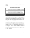
IRC2 IRC1 IRC0
000zero wait states
0X1illegal
11Xillegal
100one wait state
1 0 1 two wait states
1 1 0 three wait states
111infinite
If you choose the infinite wait states option, you must keep P5.6
configured as the READY signal. Also, be sure to add external hardware
to count wait states and pull READY high within a specified time.
Otherwise, a defective external device could tie up the address/data bus
indefinitely.
0 0 Reserved; for compatibility with future devices, write zero to this bit.
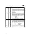
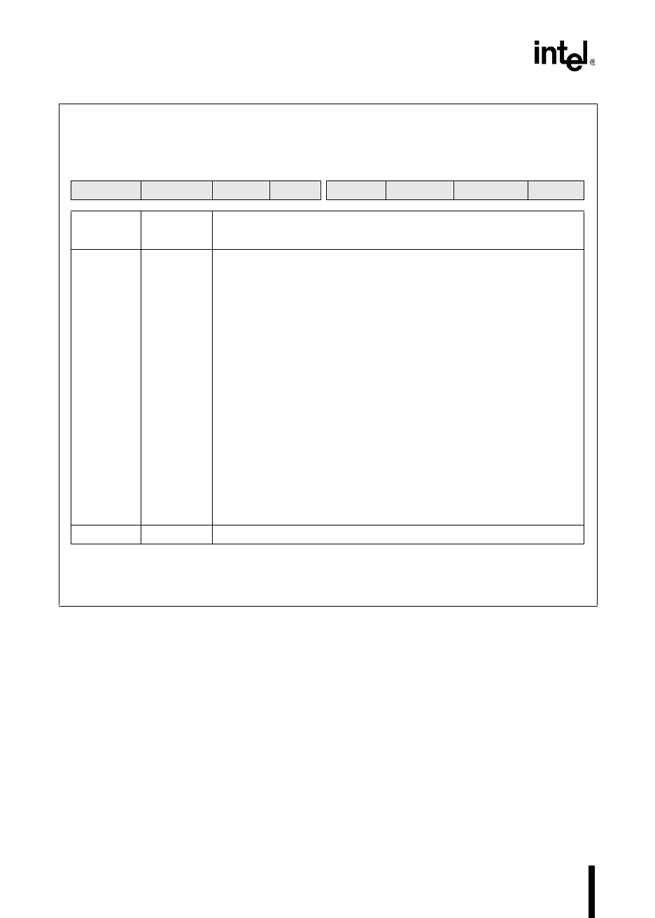
CCR1 (Continued)
no direct access
†
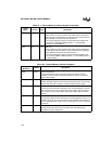
The chip configuration 1 (CCR1) register enables the watchdog timer and selects the bus timing
mode. Two of its bits combine with three bits of CCR0 to control wait states and bus width.
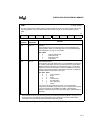
7 0
1 1 0 1 WDE BW1 IRC2 0
Bit
Number
Bit
Mnemonic
Function
†
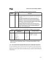
The CCRs are loaded with the contents of the chip configuration bytes (CCBs) after reset, unless
the microcontroller is entering programming modes (see “Entering Programming Modes” on page
16-13), in which case the programming chip configuration bytes (PCCBs) are used. The CCBs
reside in nonvolatile memory at addresses 2018H (CCB0) and 201AH (CCB1).
Figure 15-2. Chip Configuration 1 (CCR1) Register