


8XC196MC, MD, MH USER’S MANUAL
12-2
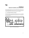
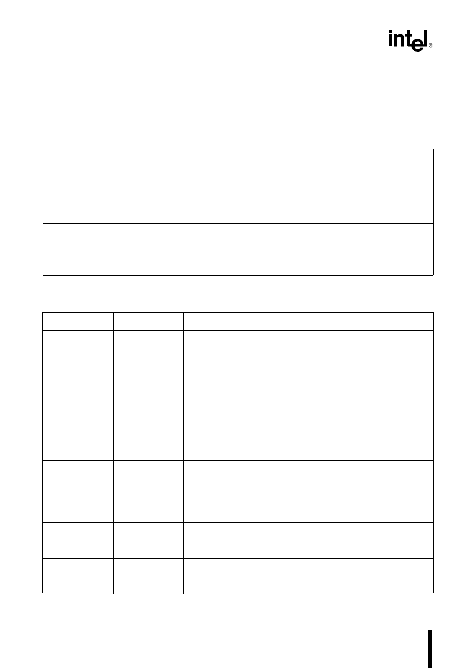
12.2 A/D CONVERTER SIGNALS AND REGISTERS
Table 12-1 lists the A/D signals and Table 12-2 describes the control and status registers. Al-
though the analog inputs are multiplexed with I/O port pins, no configuration is necessary.
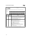
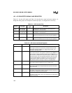
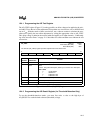
Table 12-1. A/D Converter Pins
Port Pin A/D Signal
A/D Signal
Type
Description
P1.4:0
P1.5:0
ACH12:8 (MC)
ACH13:8 (MD)
I Analog inputs. See the “Voltage on Analog Input Pin”
specification in the datasheet.
P0.7:0 ACH7:0
(MC, MD, MH)
I Analog inputs. See the “Voltage on Analog Input Pin”
specification in the datasheet.
— ANGND GND Reference Ground
Must be connected for A/D converter and port operation.
—V
REF
PWR Reference Voltage
Must be connected for A/D converter and port operation.
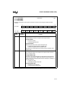
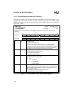
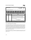
Table 12-2. A/D Control and Status Registers
Mnemonic Address Description
AD_COMMAND 1FACH A/D Command
This register selects the A/D channel, controls whether the A/D
conversion starts immediately or is triggered by the EPA, and
selects the operating mode.
AD_RESULT 1FAAH, 1FABH A/D Result
For an A/D conversion, the high byte contains the eight MSBs from
the conversion, while the low byte contains the two LSBs from a 10-
bit conversion (undefined for an 8-bit conversion), indicates which
A/D channel was used, and indicates whether the channel is idle.
For a threshold-detection, calculate the value for the successive
approximation register and write that value to the high byte of
AD_RESULT. Clear the low byte or leave it in its default state.
AD_TEST 1FAEH A/D Conversion Test
This register specifies adjustments for zero-offset errors.
AD_TIME 1FAFH A/D Conversion Time
This register defines the sample window time and the conversion
time for each bit.
INT_MASK 0008H Interrupt Mask
The AD bit in this register enables or disables the A/D interrupt. Set
the AD bit to enable the interrupt request.
INT_PEND 0009H Interrupt Pending
The AD bit in this register, when set, indicates that an A/D interrupt
request is pending.