8XC196MC, MD, MH USER’S MANUAL
13-4
13.2 APPLYING AND REMOVING POWER
When power is first applied to the device, RESET# must remain continuously low for at least one
state time after the power supply is within tolerance and the oscillator/clock has stabilized; oth-
erwise, operation might be unpredictable. Similarly, when powering down a system, RESET#
should be brought low before V
CC
is removed; otherwise, an inadvertent write to an external lo-
cation might occur. Carefully evaluate the possible effect of power-up and power-down sequenc-
es on a system.
13.3 NOISE PROTECTION TIPS
The fast rise and fall times of high-speed CMOS logic often produce noise spikes on the power
supply lines and outputs. To minimize noise, it is important to follow good design and board lay-
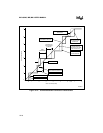
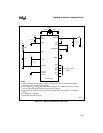
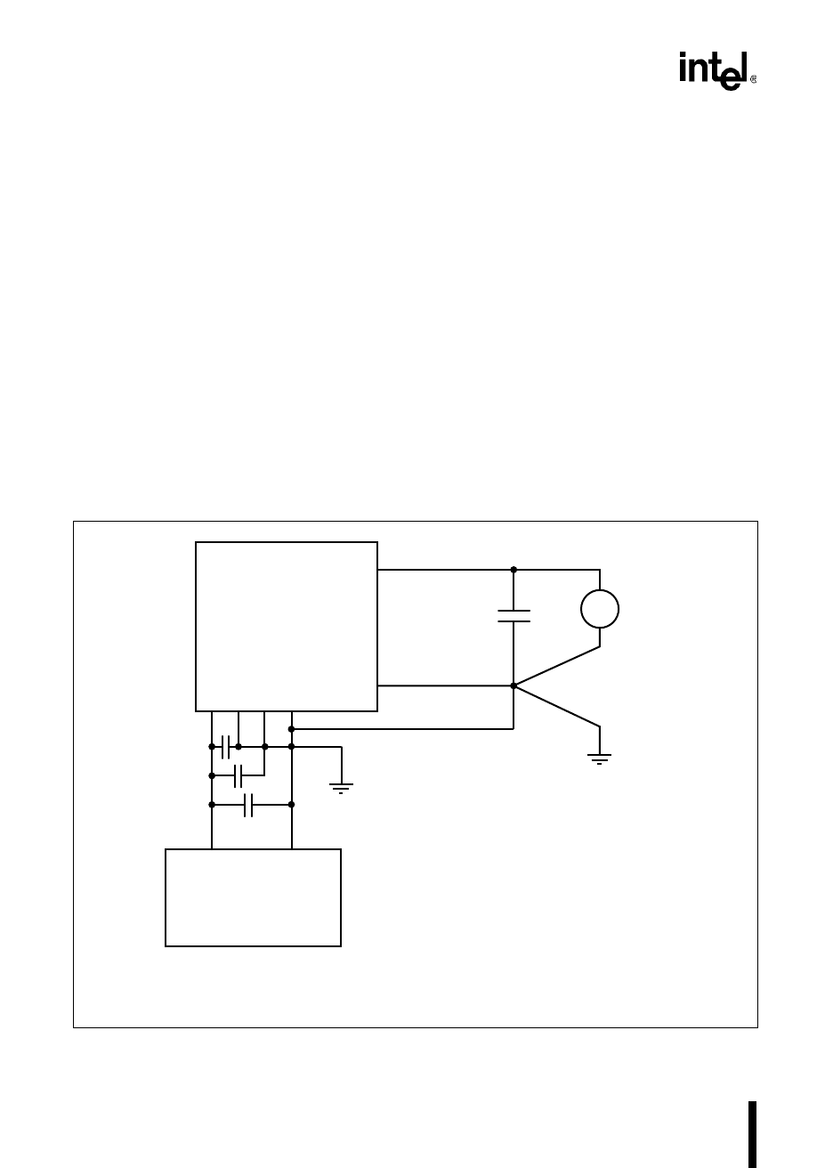
out techniques. We recommend liberal use of decoupling capacitors and transient absorbers. Add
0.01 µF bypass capacitors between V
CC
and each V
SS
pin and a 1.0 µF capacitor between V
REF
and
ANGND to reduce noise (Figure 13-2). Place the capacitors as close to the device as possible.
Use the shortest possible path to connect V
SS
lines to ground and each other.
Figure 13-2. Power and Return Connections
8XC196 Device
V
REF
ANGND
+5 V 5 V
Return
Analog
Ground
Plane
Power Source
†
†
†
Use 0.01 µF bypass capacitors for maximum decoupling.
Digital
Ground
Plane
+
1.0 µF
A0272-02
+
–
V
REF
V
CC
V
SS
V
SS
V
SS
†


