12-17
ANALOG-TO-DIGITAL (A/D) CONVERTER
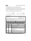
Differential nonlinearity is the degree to which actual code widths differ from the ideal one-LSB
width. It provides a measure of how much the input voltage may have changed in order to produce
a one-count change in the conversion result. In the 10-bit converter, the code widths are ideally
5 mV (V
REF
/ 1024). If such a converter is specified to have a maximum differential nonlinearity
of 2 LSBs (10 mV), the maximum code width will be no greater than 10 mV larger than ideal, or
15 mV.
Because the A/D converter has no missing codes, the minimum code width will always be greater
than –1 (negative one). The differential nonlinearity error on a particular code width is compen-
sated for by other code widths in the transfer function, such that 1024 unique steps occur. The
actual code widths in this converter typically vary from 2.5 mV to 7.5 mV.
Nonlinearity is the worst-case deviation of code transitions from the corresponding code transi-
tions of the ideal characteristic. Nonlinearity describes the extent to which differential nonlinear-
ities can add up to produce an overall maximum departure from a linear characteristic. If the
differential nonlinearity errors are too large, it is possible for an A/D converter to miss codes or
to exhibit non-monotonic behavior. Neither behavior is desirable in a closed-loop system. A con-
verter has no missing codes if there exists for each output code a unique input voltage range that
produces that code only. A converter is monotonic if every subsequent code change represents an
input voltage change in the same direction.
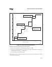
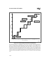
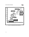
Differential nonlinearity and nonlinearity are quantified by measuring the terminal-based linear-
ity errors. A terminal-based characteristic results when an actual characteristic is translated and
scaled to eliminate zero-offset and full-scale error, as shown in Figure 12-11. The terminal-based
characteristic is similar to the actual characteristic that would result if zero-offset and full-scale
error were externally trimmed away. In practice, this is done by using input circuits that include
gain and offset trimming. In addition, V
REF
could also be closely regulated and trimmed within
the specified range to affect full-scale error.
Other factors that affect a real A/D converter system include temperature drift, failure to com-
pletely reject unwanted signals, multiplexer channel dissimilarities, and random noise. Fortunate-
ly, these effects are small. Temperature drift is the rate at which typical specifications change with
a change in temperature. These changes are reflected in the temperature coefficients. Unwanted
signals come from three main sources: noise on V
CC
, input signal changes on the channel being
converted (after the sample window has closed), and signals applied to channels not selected by
the multiplexer. The effects of these unwanted signals are specified as Vcc rejection, off-isolation,
and feedthrough, respectively. Finally, multiplexer on-channel resistances differ slightly from one
channel to the next, which causes channel-to-channel matching errors and repeatability errors.
Differences in DC leakage current from one channel to another and random noise in general con-
tribute to repeatability errors.


