8XC196MC, MD, MH USER’S MANUAL
16-32
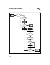
Assert PALE# to begin programming. The algorithm sends five programming pulses that write
the port 3 data to the OTPROM, then it compares the input data with the programmed data. If the
programming verifies, the PVER signal lights the LED to indicate successful programming. Oth-
erwise, you can pulse PALE# to repeat programming. Complete the procedure by following the
power-down sequence (page 16-14).
NOTE
The PCCB and UPROM programming modes are available only for the
8XC196MH device. The pulse width is 200 µs at 8 MHz or 266 µs at 6 MHz.
16.11 RUN-TIME PROGRAMMING
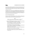
You can program an OTPROM location during normal code execution. To make the OTPROM
array accessible, apply V
CC
voltage to EA# while you reset the device. Apply V
PP
voltage to the
V
PP
pin during the entire programming process. Then simply write to the location to be pro-
grammed.
NOTE
Programming either security-lock bit in CCB0 disables run-time
programming. (For details, see “Controlling Access to the OTPROM During
Normal Operation” on page 16-4.)
Immediately after writing to the OTPROM, the device must either enter idle mode or execute
code from external memory. An access to OTPROM would abort the current programming cycle.
Each programming cycle begins when a word is written to the OTPROM and ends when the next
OTPROM access occurs. Each word requires a total of five programming cycles, each of which
must be approximately 100 µs in duration.
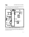
Figure 16-15 is a run-time programming example. It performs five programming cycles for each
word. After each programming cycle, the code causes the device to enter idle mode.
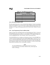
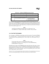
Table 16-13. PCCB and UPROM Programming Values
Pins PCCB Programming UPROM Programming
PMODE3:0 0DH 09H
P4.7:0 FFH FFH
P3.7:0 Data to be programmed in PCCB
(See CCR descriptions in Appendix C)
Value to program UPROM bits:
04H to program DED only
08H to program DEI only
0CH to program both DED and DEI


