8XC196MC, MD, MH USER’S MANUAL
6-12
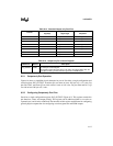
6.3.4 Bidirectional Port Considerations
This section outlines special considerations for using the pins of these ports.
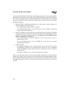
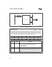
Port 1 (8XC196MH) After reset, your software must configure the device to match the
external system. This is accomplished by writing appropriate config-
uration data into P1_MODE. Writing to P1_MODE not only
configures the pins but also turns off the transistor that weakly holds
the pins high (Q4 in Figure 6-2 on page 6-8). For this reason, even if
port 1 is to be used as it is configured at reset, you should still write
data into P1_MODE.
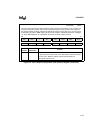
Port 2 After reset, your software must configure the device to match the
external system. This is accomplished by writing appropriate config-
uration data into P2_MODE. Writing to P2_MODE not only
configures the pins but also turns off the transistor that weakly holds
the pins high (Q4 in Figure 6-2 on page 6-8). For this reason, even if
port 2 is to be used as it is configured at reset, you should still write
data into P2_MODE.
P2.7 A value written to P2_REG.7 is held in a buffer until P2_MODE.7 is
cleared, at which time the value is loaded into P2_REG.7. A value
read from P2_REG.7 is the value currently in the register, not the
value in the buffer. Therefore, any change to P2_REG.7 can be read
only after P2_MODE.7 is cleared.
Port 5 After reset, the device configures port 5 to match the external system.
The following paragraphs describe the states of the port 5 pins after
reset and until your software writes to the P5_MODE register.
Writing to P5_MODE not only configures the pins but also turns off
the transistor that weakly holds the pins high (Q4 in Figure 6-2 on
page 6-8). For this reason, even if port 5 is to be used as it is
configured at reset, you should still write data into P5_MODE.
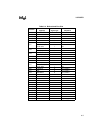
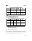
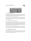
Table 6-10. Port Pin States After Reset and After Example Code Execution
Action or Code
Resulting Pin States
†
P
x
.7 P
x
.6 P
x
.5 P
x
.4 P
x
.3 P
x
.2 P
x
.1 P
x
.0
Reset wk1 wk1 wk1 wk1 wk1 wk1 wk1 wk1
LDB P
x
_DIR, #00011111B 1 1 1 wk1 wk1 wk1 wk1 wk1
LDB P
x
_MODE, #00000000B 1 1 1 HZ1 HZ1 HZ1 HZ1 HZ1
LDB P
x
_REG, #10010011B 1 0 0 HZ1 0 0 HZ1 HZ1
†
wk1 = weakly pulled high, HZ1 = high impedance (actually a “1” with an external pull-up).


