8XC196MC, MD, MH USER’S MANUAL
7-2
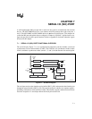
An independent, 15-bit baud-rate generator controls the baud rate of the serial port. Either XTAL1
or BCLKx can provide the clock signal for modes 0–3. In mode 4, the internal shift clock is output
on SCLKx# or an external shift clock is input on SCLKx# (in which case the baud-rate generator
is not used). The baud-rate register (SPx_BAUD) selects the clock source and the baud rate. The
serial port control register (SPx_CON) register controls whether SCLKx# outputs the internal
shift clock or inputs an external shift clock.
7.2 SERIAL I/O PORT SIGNALS AND REGISTERS
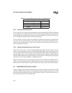
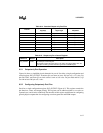
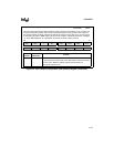
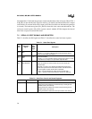
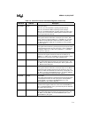
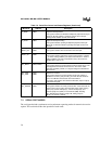
Table 7-1 describes the SIO signals and Table 7-2 describes the control and status registers.
Table 7-1. Serial Port Signals
Port
Pin
Serial Port
Signal
Serial
Port
Signal
Type
Description
P1.0
P1.2
TXD0
TXD1
O Transmit Serial Data.
In modes 1, 2, 3, and 4, TXD
x
transmits serial port output data. In
mode 0, it is the serial clock output.
P1.1
P1.3
RXD0
RXD1
I/O Receive Serial Data.
In modes 1, 2, 3, and 4, RXD
x
receives serial port input data. In mode
0, it functions as an input or an open-drain output for data.
P2.1
P2.7
SCLK0#/BCLK0
SCLK1#/BCLK1
I/O Baud Clock.
BCLK
x
can provide an external clock source for the baud-rate
generator input.
Shift Clock. In mode 4 only, SCLK
x
# are bidirectional shift clock
signals that synchronize the serial data transfer. The DIR bit in the
SP_CON register controls the direction of SCLK
x
#:
DIR = 0 causes SCLK
x
# to output the internal shift clock.
DIR = 1 allows an external shift clock to be input on SCLK
x
#.
Table 7-2. Serial Port Control and Status Registers
Mnemonic Address Description
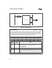
INT_MASK1 0013H Interrupt Mask 1
Setting the TI
x
bit enables the transmit interrupt; clearing the bit
disables (masks) the interrupt.
Setting the RI
x
bit enables the receive interrupt; clearing the bit
disables (masks) the interrupt.
Setting the SPE bit enables the serial port receive error interrupt.


