


C-5
REGISTERS
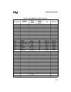
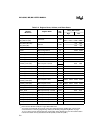
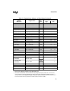
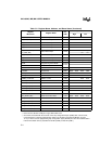
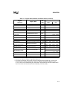
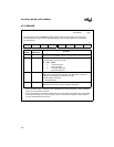
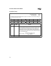
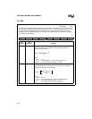
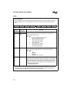
T1CONTROL Timer 1 Control 1F78 0000 0000
T2CONTROL Timer 2 Control 1F7C 0000 0000
T1RELOAD Timer 1 Reload 1F72 XXXX XXXX XXXX XXXX
TIMER1 Timer 1 Value 1F7A 0000 0000 0000 0000
TIMER2 Timer 2 Value 1F7E 0000 0000 0000 0000
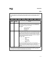
USFR (MC, MD)
USFR (MH)
UPROM Special Function 1FF6
0000 0010
XXXX XXXX
WATCHDOG Watchdog Timer 000A XXXX XXXX
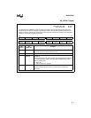
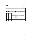
WG_COMP1 Waveform Gen Phase Comp 1 1FC2 0000 0000 0000 0000
WG_COMP2 Waveform Gen Phase Comp 2 1FC4 0000 0000 0000 0000
WG_COMP3 Waveform Gen Phase Comp 3 1FC6 0000 0000 0000 0000
WG_CONTROL (MC, MD)
WG_CONTROL (MH)
Waveform Gen Control 1FCC
0000 0000 1100 0000
1000 0000 0000 0000
WG_COUNTER Waveform Gen Count 1FCA XXXX XXXX XXXX XXXX
WG_OUTPUT Waveform Gen Output Config 1FC0 0000 0000 0000 0000
WG_PROTECT (MC, MD)
WG_PROTECT (MH)
Waveform Gen Protection 1FCE
1111 0000
1110 0000
WG_RELOAD Waveform Gen Reload 1FC8 0000 0000 0000 0000
WSR Window Selection 0014 0000 0000
ZERO_REG Zero Register 0000 0000 0000 0000 0000
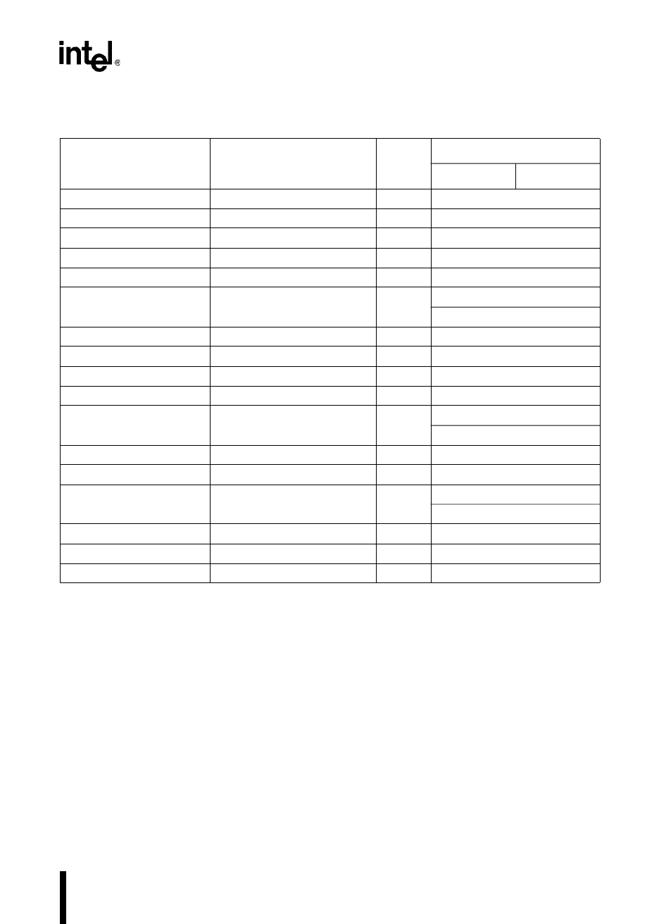
Table C-2. Register Name, Address, and Reset Status (Continued)
Register
Mnemonic
Register Name
Hex
Addr
Binary Reset Value
High Low
†
Reset value is FFH when pin is not driven.
††
Reset value is 80H if the EA# pin is high, A9H if EA# is low.
†††
The CCRs are loaded with the contents of the chip configuration bytes (CCBs) after a device reset,
unless the device is entering programming modes (see “Entering Programming Modes” on page
16-13), in which case the programming chip configuration bytes (PCCBs) are used. The CCBs reside in
internal nonvolatile memory at addresses 2018H (CCB0) and 201AH (CCB1).