


13-1
CHAPTER 13
MINIMUM HARDWARE CONSIDERATIONS
The 8XC196MC, MD, and MH have several basic requirements for operation within a system.
This chapter describes options for providing the basic requirements and discusses other hardware
considerations.
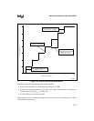
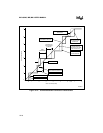
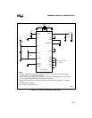
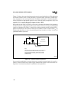
13.1 MINIMUM CONNECTIONS
Table 13-1 lists the signals that are required for the device to function and Figure 13-1 shows the
connections for a minimum configuration.
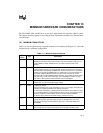
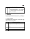
Table 13-1. Minimum Required Signals
Signal
Name
Type Description
ANGND GND Analog Ground
ANGND must be connected for A/D converter and port 0 operation (also port 1 on
the 8XC196MC and MD). ANGND and V
SS
should be nominally at the same
potential.
RESET# I/O Reset
A level-sensitive reset input to and open-drain system reset output from the micro-
controller. Either a falling edge on RESET# or an internal reset turns on a pull-down
transistor connected to the RESET# pin for 16 state times. In the powerdown and
idle modes, asserting RESET# causes the chip to reset and return to normal
operating mode. The 8XC196MH provides the option of preventing an internal reset
from generating a reset on the external pin (see “Resetting the Device” on page
13-8). After a device reset, the first instruction fetch is from 2080H.
V
CC
PWR Digital Supply Voltage
Connect each V
CC
pin to the digital supply voltage.
V
PP
PWR Programming Voltage
During programming, the V
PP
pin is typically at +12.5 V (V
PP
voltage). Exceeding the
maximum V
PP
voltage specification can damage the device.
V
PP
also causes the device to exit powerdown mode when it is driven low for at least
50 ns. Use this method to exit powerdown only when using an external clock source
because it enables the internal phase clocks, but not the internal oscillator.
On devices with no internal nonvolatile memory, connect V
PP
to V
CC
.
V
REF
PWR Reference Voltage for the A/D Converter
This pin also supplies operating voltage to both the analog portion of the A/D
converter and the logic used to read port 0 (also port 1 in the 8XC196MC and
8XC196MD).
V
SS
GND Digital Circuit Ground
Connect each V
SS
pin to ground through the lowest possible impedance path.