


8XC251SA, SB, SP, SQ USER’S MANUAL
4-8
4.5 CONFIGURING THE EXTERNAL MEMORY INTERFACE
This section describes the configuration options that affect the external memory interface. The
configuration bits described here determine the following interface features:
• page mode or nonpage mode (PAGE#)
• the number of external address pins (16, 17, or 18) (RD1:0)
• the memory regions assigned to the read signals RD# and PSEN# (RD1:0)
• the external wait states (WSA1:0#, WSB1:0#, XALE#)
• mapping a portion of on-chip code memory to data memory (EMAP#)
4.5.1 Page Mode and Nonpage Mode (PAGE#)
The PAGE# bit (UCONFIG0.1) determines whether code fetches use page mode or nonpage
mode and whether data is transmitted on P2 or P0. See Figure 13-1 on page 13-1 and section
13.2.3, “Page Mode Bus Cycles,” for a description of the bus structure and page mode operation.
• Nonpage mode: PAGE# = 1. The bus structure is the same as for the MCS 51 architecture
with data D7:0 multiplexed with A7:0 on P0. External code fetches require two state times
(4T
OSC
).
• Page mode: PAGE# = 0. The bus structure differs from the bus structure in MCS 51
controllers. Data D7:0 is multiplexed with A15:8 on P2. Under certain conditions, external
code fetches require only one state time (2T
OSC
).
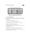
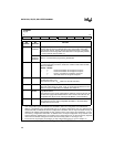
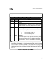
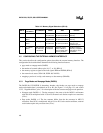
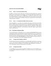
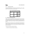
Table 4-2. Memory Signal Selections (RD1:0)
RD1:0
P1.7/CEX/
A17/WCLK
P3.7/RD#/A16 PSEN# WR# Features
0 0 A17 A16 Asserted for
all addresses
Asserted for writes to
all memory locations
256-Kbyte external
memory
0 1 P1.7/CEX4/
WCLK
A16 Asserted for
all addresses
Asserted for writes to
all memory locations
128-Kbyte external
memory
1 0 P1.7/CEX4/
WCLK
P3.7 only Asserted for
all addresses
Asserted for writes to
all memory locations
64-Kbyte external
memory. One
additional port pin.
1 1 P1.7/CEX4/
WCLK
RD# asserted
for addresses
≤ 7F:FFFFH
Asserted for
≥ 80:0000H
Asserted only for
writes to MCS 51
microcontroller data
memory locations.
64-Kbyte external
memory. Compatible
with MCS 51 micro-
controllers.