


8XC251SA, SB, SP, SQ USER’S MANUAL
4-6
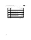
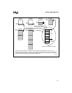
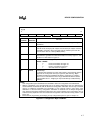
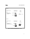
Figure 4-3. Configuration Byte UCONFIG0
UCONFIG0
(1), (3)
Address:FF:FFF8H (2)
7 0
UCON WSA1# WSA0# XALE# RD1 RD0 PAGE# SRC
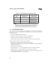
Bit
Number
Bit
Mnemonic
Function
7 UCON
87C251Sx
Configuration Byte Location Selector (OTPROM/EPROM products only):
Clearing this bit causes the 8XC251S
x
to fetch configuration information
from on-chip memory. Leaving this bit unprogrammed (logic 1) causes the
8XC251S
x
to fetch configuration information from on-chip memory if EA# =
1 or from external memory if EA# = 0.
—
80C251Sx
83C251Sx
Reserved:
Write a 1 to this bit when programming UCONFIG0.
6:5 WSA1:0#
Wait State A (all regions except 01:):
For external memory accesses, selects the number of wait states for RD#,
WR#, and PSEN#.
WSA1# WSA0#
0 0 Inserts 3 wait states for all regions except 01:
0 1 Inserts 2 wait states for all regions except 01:
1 0 Inserts 1 wait state for all regions except 01:
1 1 Zero wait states for all regions except 01:
4 XALE# Extend ALE:
Set this bit for ALE = T
OSC
.
Clear this bit for ALE = 3T
OSC
(adds one external wait state).
3:2 RD1:0 Memory Signal Selection:
RD1:0 bit codes specify an 18-bit, 17-bit, or 16-bit external address bus and
address ranges for RD#, WR#, and PSEN#. See Table 4-2.
1 PAGE# Page Mode Select:
Clear this bit for page mode enabled with A15:8/D7:0 on P2 and A7:0 on P0.
Set this bit for page mode disabled with A15:8 on P2 and A7:0/D7:0 on P0
(compatible with 44-pin PLCC and 40-pin DIP MCS 51 microcontrollers).
0 SRC Source Mode/Binary Mode Select:
Clear this bit for binary mode (compatible with MCS 51 microcontrollers).
Set this bit for source mode.
NOTES:
1. User configuration bytes UCONFIG0 and UCONFIG1 define the configuration of the 8XC251S
x
.
2. Address. UCONFIG0 is the second-lowest byte of the 8-byte configuration array. As determined by
UCON and EA#, the 8XC251S
x
fetches configuration information from on-chip nonvolatile memory at
addresses FF:FFF8H and FF:FFF9H or from external memory using these same addresses. In exter-
nal memory, configuration information is obtained from an 8-byte configuration array located at the
highest addresses implemented. The location of the configuration array in external memory depends
on the size and decode arrangement of the external memory (Table 4-1 and Figure 4-2).
3. Instructions for programming and verifying on-chip configuration bytes are given in Chapter 14.