


8XC251SA, SB, SP, SQ USER’S MANUAL
9-4
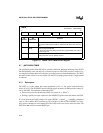
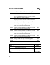
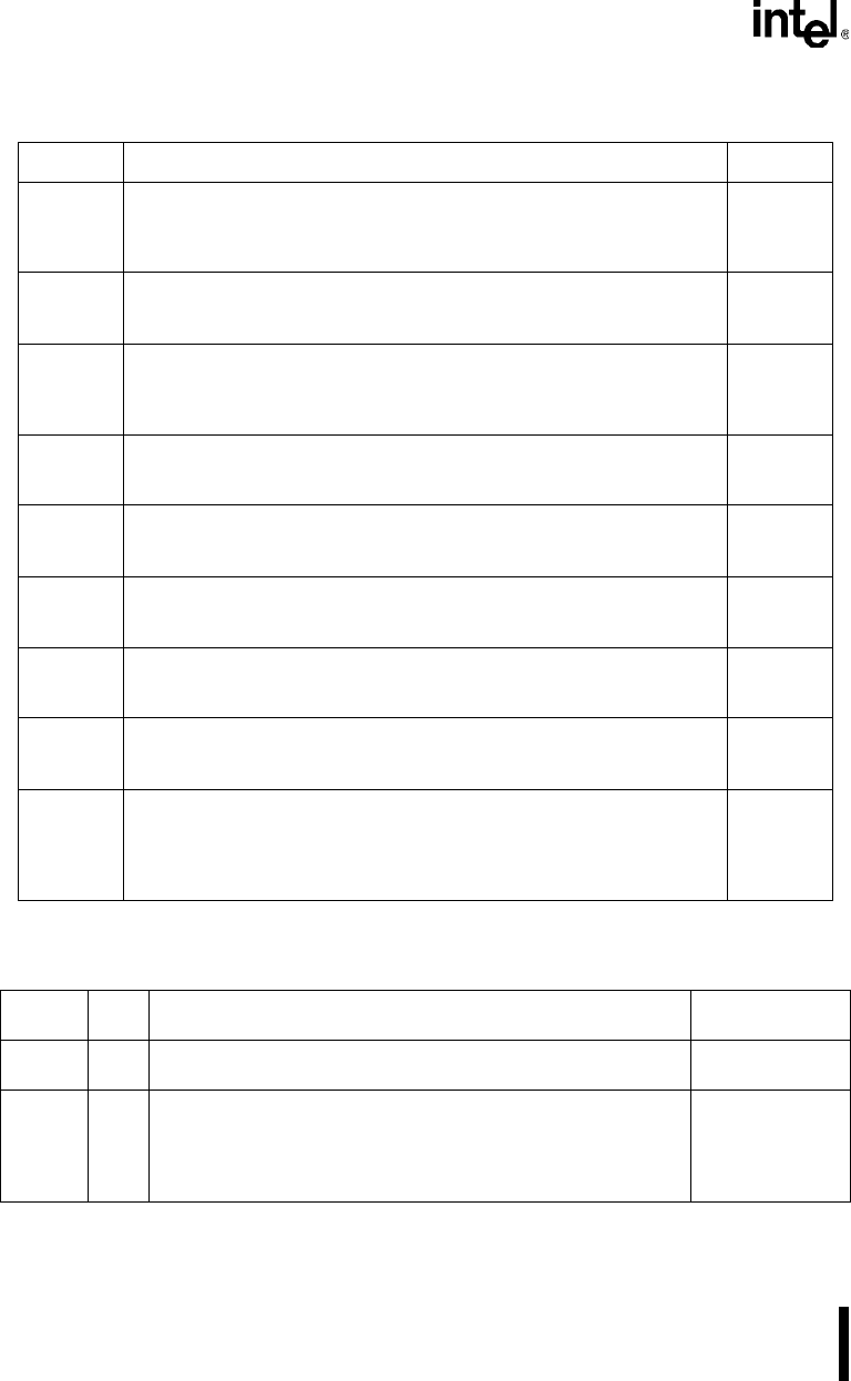
Table 9-1. PCA Special Function Registers (SFRs)
Mnemonic Description Address
CL
CH
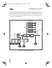
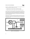
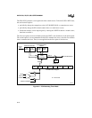
PCA Timer/Counter. These registers serve as a common 16-bit timer or
event counter for the five compare/capture modules. Counts F
OSC
/12,
F
OSC
/4, timer 0 overflow, or the external signal on P1.2/ECI, as selected by
CMOD. In PWM mode CL operates as an 8-bit timer.
S:E9H
S:F9H
CCON PCA Timer/Counter Control Register. Contains the run control bit and
the overflow flag for the PCA timer/counter, and interrupt flags for the five
compare/capture modules.
S:D8H
CMOD PCA Timer/Counter Mode Register. Contains bits for disabling the PCA
timer/counter during idle mode, enabling the PCA watchdog timer (module
4), selecting the timer/counter input, and enabling the PCA timer/counter
overflow interrupt.
S:D9H
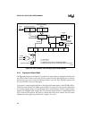
CCAP0H
CCAP0L
PCA Module 0 Compare/Capture Registers. This register pair stores the
comparison value or the captured value. In the PWM mode, the low-byte
register controls the duty cycle of the output waveform.
S:FAH
S:EAH
CCAP1H
CCAP1L
PCA Module 1 Compare/Capture Registers. This register pair stores the
comparison value or the captured value. In the PWM mode, the low-byte
register controls the duty cycle of the output waveform.
S:FBH
S:EBH
CCAP2H
CCAP2L
PCA Module 2 Compare/Capture Registers. This register pair stores the
comparison value or the captured value. In the PWM mode, the low-byte
register controls the duty cycle of the output waveform.
S:FCH
S:ECH
CCAP3H
CCAP3L
PCA Module 3 Compare/Capture Registers. This register pair stores the
comparison value or the captured value. In the PWM mode, the low-byte
register controls the duty cycle of the output waveform.
S:FDH
S:EDH
CCAP4H
CCAP4L
PCA Module 4 Compare/Capture Registers. This register pair stores the
comparison value or the captured value. In the PWM mode, the low-byte
register controls the duty cycle of the output waveform.
S:FEH
S:EEH
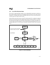
CCAPM0
CCAPM1
CCAPM2
CCAPM3
CCAPM4
PCA Compare/Capture Module Mode Registers. Contain bits for
selecting the operating mode of the compare/capture modules and
enabling the compare/capture flag. See Table 9-3 on page 9-14
for mode
select bit combinations.
S:DAH
S:DBH
S:DCH
S:DDH
S:DEH
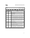
Table 9-2. External Signals
Signal
Name
Type Description
Alternate
Function
ECI I PCA Timer/counter External Input. This signal is the external
clock input for the PCA timer/counter.
P1.2
CEX0
CEX1
CEX2
CEX3
CEX4
I/O Compare/Capture Module External I/O. Each compare/capture
module connects to a Port 1 pin for external I/O. When not used by
the PCA, these pins can handle standard I/O.
P1.3
P1.4
P1.5
P1.6/WAIT#
P1.7/A17/WCLK