


8XC251SA, SB, SP, SQ USER’S MANUAL
3-12
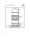
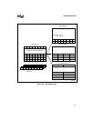
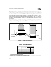
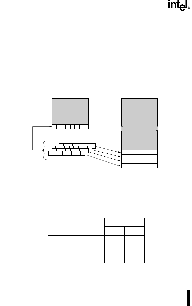
Register file locations 0–7 actually consist of four switchable banks of eight registers each, as il-
lustrated in Figure 3-7. The four banks are implemented as the first 32 bytes of on-chip RAM and
are always accessible as locations 00:0000H–00:001FH in the memory address space.† Only one
of the four banks is accessible via the register file at a given time. The accessible, or “active,”
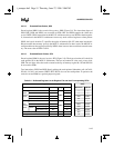
bank is selected by bits RS1 and RS0 in the PSW register, as shown in Table 3-3. (The PSW is
described in “Program Status Words” on page 5-16.) This bank selection can be used for fast con-
text switches.
Register file locations 8–31 and 56–63 are always accessible. These locations are implemented
as registers in the CPU. Register file locations 32–55 are reserved and cannot be accessed.
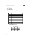
Figure 3-7. Register File Locations 0–7
† Because these locations are dedicated to the register file, they are not considered a part of the general-
purpose, 1-Kbyte, on-chip RAM (locations 00:0020H–00:041FH).
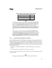
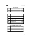
Table 3-3. Register Bank Selection
Bank Address Range
PSW Selection Bits
RS1 RS0
Bank 0 00H–07H 0 0
Bank 1 08H–0FH 0 1
Bank 2 10H–17H 1 0
Bank 3 18H–1FH 1 1
A4215-01
Register File
01234567
8
63
Memory Address Space
FF:FFFFH
00:0020H
18H 1FH
10H 17H
08H 0FH
00H 07H
Banks 0–3
0 1234567
01234567
01234567
01234567
PSW bits RS1:0
select one bank
to be accessed via
the register file.
Banks 0–3
accessible
in memory
address space