


8XC251SA, SB, SP, SQ USER’S MANUAL
4-2
For ROM/OTPROM/EPROM devices, user configuration bytes UCONFIG0 and UCONFIG1
can be programmed at the factory or on-site using the procedures provided in Chapter 14, “Pro-
gramming and Verifying Nonvolatile Memory.” For devices without ROM/OTPROM/ EPROM,
the designer should store configuration information in an eight-byte configuration array located
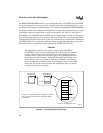
at the highest addresses implemented in external code memory. See Table 4-1 and Figure 4-2.
Bit definitions of UCONFIG0 and UCONFIG1 are provided in Figures 4-3 and 4-4. The upper 6
bytes of the configuration array are reserved for future use. When EA# = 1, the 8XC251Sx obtains
configuration information at reset from on-chip non-volatile memory at addresses FF:FFF8H and
FF:FFF9H. When EA# = 0, the microcontroller obtains configuration information at reset from
the external memory system using internal addresses FF:FFF8H and FF:FFF9H.
CAUTION
The eight highest addresses in the memory address space (FF:FFF8H–
FF:FFFFH) are reserved for the configuration array. Do not read or write these
locations. These addresses are also used to access the configuration array in
external memory, so the same restrictions apply to the eight highest addresses
implemented in external memory. Instructions that might inadvertently cause
these addresses to be accessed due to call returns or prefetches should not be
located at addresses immediately below the configuration array. Use an EJMP
instruction, five or more addresses below the configuration array, to continue
execution in other areas of memory.
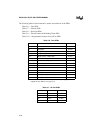
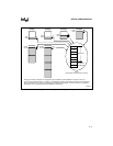
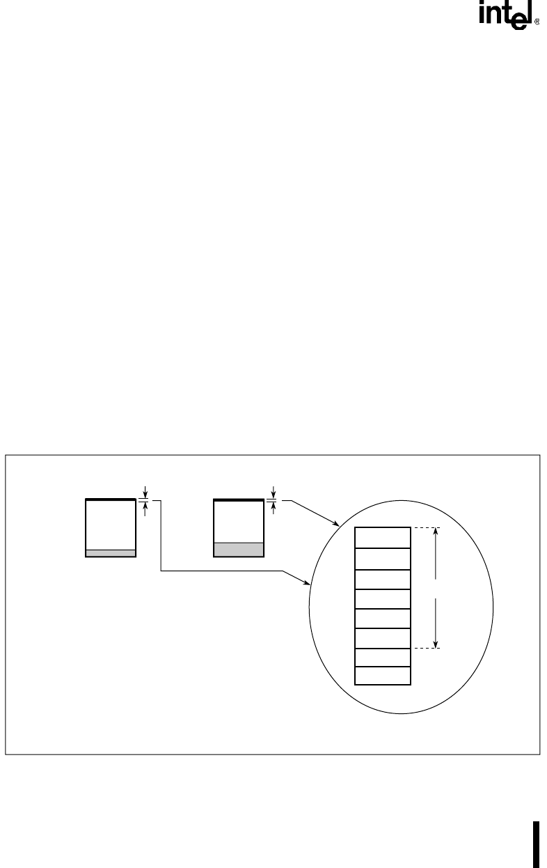
Figure 4-1. Configuration Array (On-chip)
A4237-01
83C251SB, SQ
87C251SB, SQ
For EA# = 1, the 8XC251S
x
obtains configuration information
from on-chip nonvolatile memory at addresses FF:FFF8H
and FF:FFF9H.
83C251SA, SP
87C251SA, SP
8 Kbytes
16 Kbytes
FF:FFFFH
FF:FFFEH
FF:FFFDH
FF:FFFCH
FF:FFFBH
FF:FFFAH
FF:FFF9H
FF:FFF8H
UCONFIG1
UCONFIG0
Reserved
Detail. On-chip configuration array.
FF:FF: