


8XC251SA, SB, SP, SQ USER’S MANUAL
7-8
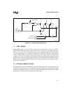
The 8XC251Sx CPU writes FFH to the P0 register for all external memory bus cycles. This over-
writes previous information in P0. In contrast, the P2 register is unmodified for external bus cy-
cles. When address bits or data bits are not on the port 2 pins, the bit values in P2 appear on the
port 2 pins.
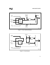
In nonpage mode, port 0 uses a strong internal pullup FET to output ones or a strong internal pull-
down FET to output zeros for the lower address byte and the data. Port 0 is in a high-impedance
state for data input.
In page mode, port 0 uses a strong internal pullup FET to output ones or a strong internal pull-
down FET to output zeros for the lower address byte; port 0 also uses a strong internal pulldown
FET to output zeros for the upper address byte.
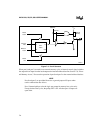
In nonpage mode, port 2 uses a strong internal pullup FET to output ones or a strong internal pull-
down FET to output zeros for the upper address byte. In page mode, port 2 uses a strong internal
pullup FET to output ones or a strong internal pulldown FET to output zeros for the upper address
byte and data. Port 2 is in a high-impedance state for data input.
NOTE
In external bus mode port 0 outputs do not require external pullups.
There are two types of external memory accesses: external program memory and external data
memory (see Chapter 13, “External Memory Interface”). External program memories utilize sig-
nal PSEN# as a read strobe. MCS 51 microcontrollers use RD# (read) or WR# (write) to strobe
memory for data accesses. Depending on its RD1:0 configuration bits, the 8XC251Sx uses
PSEN# or RD# for data reads (see section 4.5.2, “Configuration Bits RD1:0”).
During instruction fetches, external program memory can transfer instructions with 16-bit ad-
dresses for binary-compatible code or with the external bus configured for extended memory ad-
dressing (17-bit or 18-bit).
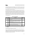
External data memory transfers use an 8-, 16-, 17-, or 18-bit address bus, depending on the in-
struction and the configuration of the external bus. Table 7-2 lists the instructions that can be used
for these bus widths.