8XC251SA, SB, SP, SQ USER’S MANUAL
13-2
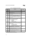
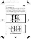
Table 13-1. External Memory Interface Signals
Signal
Name
Type Description
Alternate
Function
A17 O Address Line 17. P1.7/CEX4/WCLK
A16 O Address Line 16. See RD#. P3.7/RD#
A15:8
†
O Address Lines. Upper address for external bus (non-page mode). P2.7:0
AD7:0
†
I/O Address/Data Lines. Multiplexed lower address and data for the
external bus (non-page mode).
P0.7:0
ALE O Address Latch Enable. ALE signals the start of an external bus
cycle and indicates that valid address information is available on
lines A15:8 and AD7:0.
PROG#
EA# I External Access. For EA# strapped to ground, all program
memory accesses are off-chip. For EA# = strapped to V
CC
, an
access is to on-chip OTPROM/ROM if the address is within the
range of the on-chip OTPROM/ROM; otherwise the access is off-
chip. The value of EA# is latched at reset. For a ROMless device,
strap EA# to ground.
V
PP
PSEN# O Program Store Enable. Read signal output. This output is
asserted for a memory address range that depends on bits RD0
and RD1 in the configuration byte (see also RD#):
RD1 RD0 Address Range for Assertion
0 0 All addresses
0 1 All addresses
1 0 All addresses
1 1 All addresses ≥ 80:0000H
—
RD# O Read or 17th Address Bit (A16). Read signal output to external
data memory or 17th external address bit (A16), depending on the
values of bits RD0 and RD1 in configuration byte. (See PSEN#):
RD1 RD0 Function
0 0 The pin functions as A16 only.
0 1 The pin functions as A16 only.
1 0 The pin functions as P3.7 only.
1 1 RD# asserted for reads at all addresses ≤7F:FFFFH.
P3.7/A16
WAIT# I Real-time Wait State Input. The real-time WAIT # input is
enabled by writing a logical ‘1’ to the WCON.0 (RTWE) bit at
S:A7H. During bus cycles, the external memory system can signal
‘system ready’ to the microcontroller in real time by controlling the
WAIT# input signal on the port 1.6 input.
P1.6/CEX3
WCLK O Wait Clock Output. The real-time WCLK output is driven at port
1.7 (WCLK) by writing a logical ‘1’ to the WCON.1 (RTWCE) bit at
S:A7H. When enabled, the WCLK output produces a square wave
signal with a period of one-half the oscillator frequency.
A17/P1.7/CEX4
WR# O Write. Write signal output to external memory. WR# is asserted for
writes to all valid memory locations.
P3.6
†
If the chip is configured for page-mode operation, port 0 carries the lower address bits (A7:0), and port 2
carries the upper address bits (A15:8) and the data (D7:0).


