


14-5
PROGRAMMING AND VERIFYING NONVOLATILE MEMORY
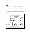
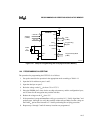
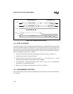
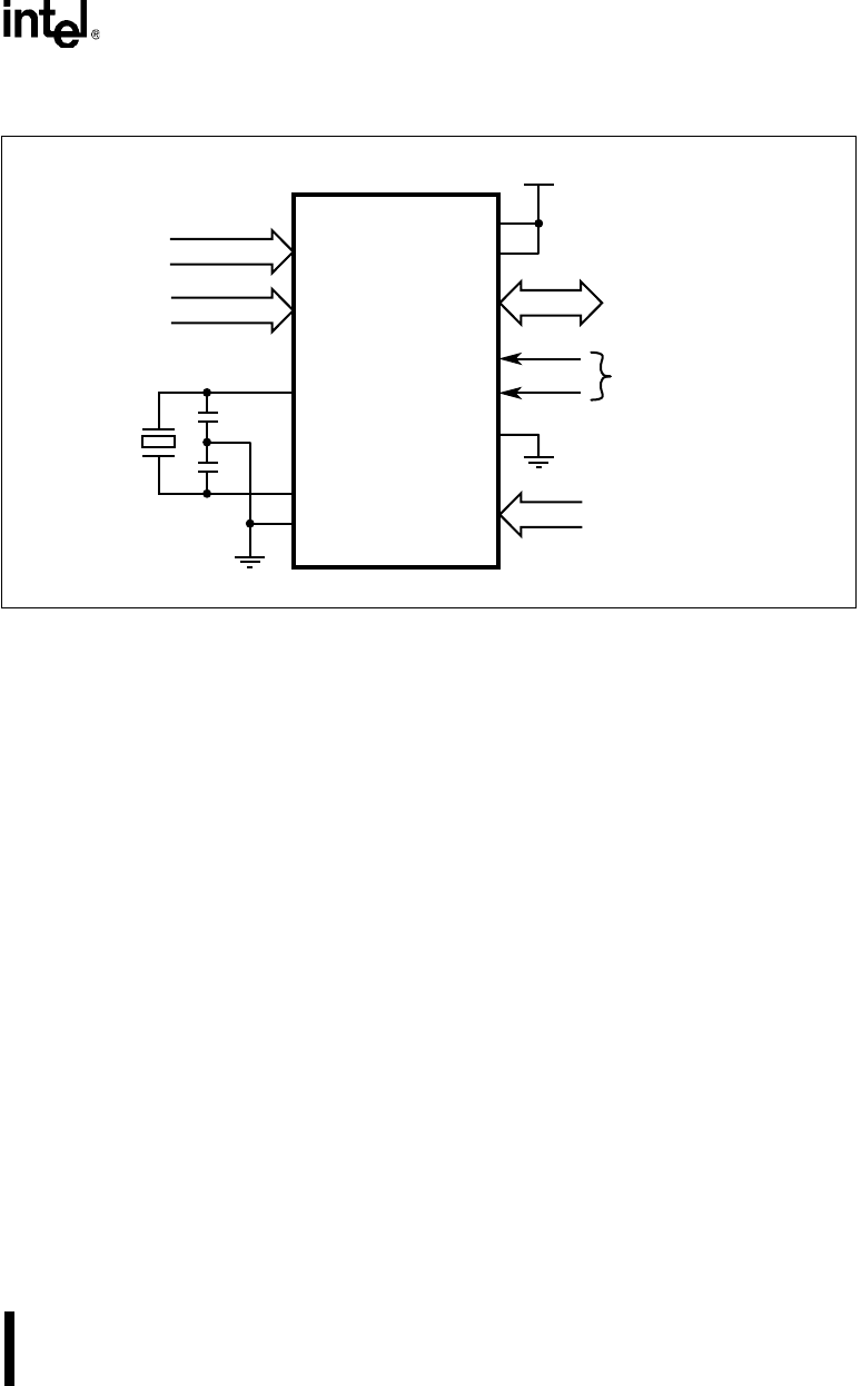
Figure 14-1. Setup for Programming and Verifying Nonvolatile Memory
14.4 PROGRAMMING ALGORITHM
The procedure for programming the 87C251Sx is as follows:
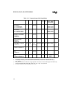
1. Set up the controller for operation in the appropriate mode according to Table 14-1.
2. Input the 16-bit address on ports 1 and 3.
3. Input the data byte on port 2.
4. Raise the voltage on the V
PP
pin from 5 V to 12.75 V.
5. Pulse the PROG# pin 5 times for the on-chip code memory and the configuration bytes,
and 25 times for the encryption array and the lock bits.
6. Reduce the voltage on the V
PP
pin to 5 V.
7. If the procedure is program/immediate-verify, go to section 14.5, “Verify Algorithm,” and
perform steps 1 through 4 to verify the currently addressed byte. Make sure the voltage on
the EA#/V
PP
pin has been lowered to 5 V before performing the verifying procedure.
8. Repeat steps 1 through 7 until all memory locations are programmed.
P0
PSEN#
ALE/PROG#
EA#/V
pp
8XC251S
x
A4122-02
4 MHz
to
6 MHz
XTAL2
A0 - A7
A8 - A15
P3
P1
Data
(8 Bits)
V
SS
V
CC
V
CC
XTAL1
Programming
Signals
Address
(16 Bits)
Program/Verify Mode
(8 Bits)
P2
RST