


C-21
REGISTERS
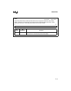
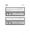
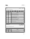
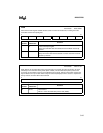
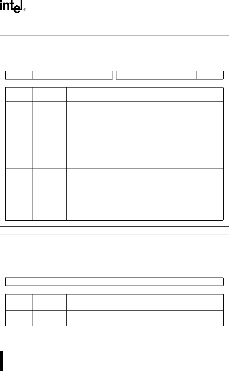
PSW1
Address: S:D1H
Reset State: 0000 0000B
Program Status Word 1. PSW1 contains bits that reflect the results of operations and bits that select
the register bank for registers R0–R7.
7 0
CY AC N RS1 RS0 OV Z —
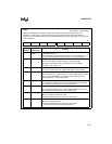
Bit
Number
Bit
Mnemonic
Function
7 CY Carry Flag:
Identical to the CY bit in the PSW register.
6 AC Auxiliary Carry Flag:
Identical to the AC bit in the PSW register.
5 N Negative Flag:
This bit is set if the result of the last logical or arithmetic operation was
negative. Otherwise it is cleared.
4:3 RS1:0 Register Bank Select Bits 0 and 1:
Identical to the RS1:0 bits in the PSW register.
2 OV Overflow Flag:
Identical to the OV bit in the PSW register.
1 Z Zero Flag:
This flag is set if the result of the last logical or arithmetic operation is
zero. Otherwise it is cleared.
0 — Reserved:
The value read from this bit is indeterminate. Write a zero to this bit.
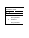
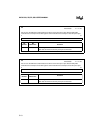
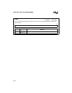
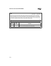
RCAP2H, RCAP2L
Address: RCAP2H S:CBH
RCAP2L S:CAH
Reset State: 0000 0000B
Timer 2 Reload/Capture Registers. This register pair stores 16-bit values to be loaded into or captured
from the timer register (TH2/TL2) in timer 2.
7 0
High/Low Byte of Timer 2 Reload/Capture Value
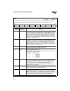
Bit
Number
Bit
Mnemonic
Function
7:0 RCAP2H.7:0
RCAP2L.7:0
High byte of the timer 2 reload/recapture register
Low byte of the timer 2 reload/recapture register