


8XC251SA, SB, SP, SQ USER’S MANUAL
13-16
13.7 PORT 0 AND PORT 2 STATUS
This section summarizes the status of the port 0 and port 2 pins when these ports are used as the
external bus. A more comprehensive description of the ports and their use is given in Chapter 7,
“Input/Output Ports.”
When port 0 and port 2 are used as the external memory bus, the signals on the port pins can orig-
inate from three sources:
• the 8XC251Sx CPU (address bits, data bits)
• the port SFRs: P0 and P2 (logic levels)
• an external device (data bits)
The port 0 pins (but not the port 2 pins) can also be held in a high-impedance state. Table 13-3
lists the status of the port 0 and port 2 pins when the chip in is the normal operating mode and the
external bus is idle or executing a bus cycle.
13.7.1 Port 0 and Port 2 Pin Status in Nonpage Mode
In nonpage mode, the port pins have the same signals as those on the 8XC51FX. For an external
memory instruction using a 16-bit address, the port pins carry address and data bits during the bus
cycle. However, if the instruction uses an 8-bit address (e.g., MOVX @Ri), the contents of P2 are
driven onto the pins. These pin signals can be used to select 256-bit pages in external memory.
During a bus cycle, the CPU always writes FFH to P0, and the former contents of P0 are lost. A
bus cycle does not change the contents of P2. When the bus is idle, the port 0 pins are held at high
impedance, and the contents of P2 are driven onto the port 2 pins.
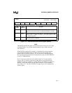
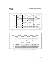
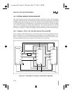
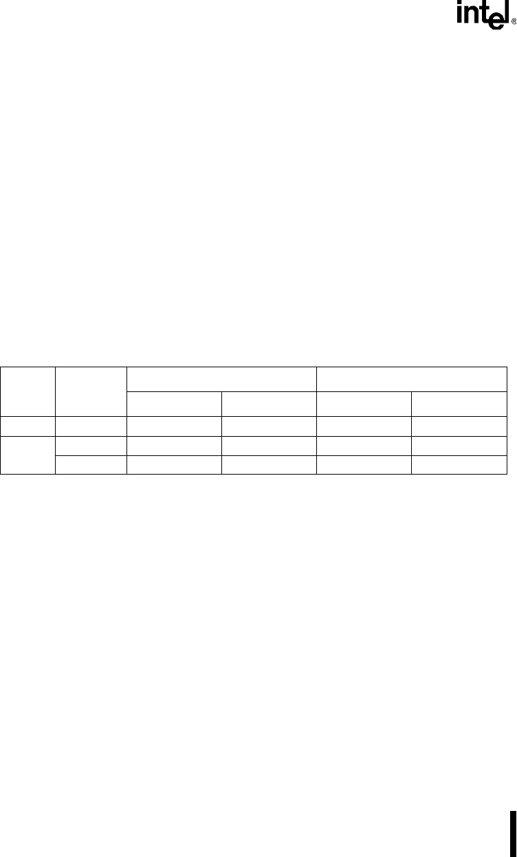
Table 13-3. Port 0 and Port 2 Pin Status In Normal Operating Mode
Port
8-bit/16-bit
Addressing
Nonpage Mode Page Mode
Bus Cycle Bus Idle Bus Cycle Bus Idle
Port 0 8 or 16 AD7:0 (1) High Impedance A7:0 (1) High Impedance
Port 2
8 P2 (2) P2 P2/D7:0 (2) High Impedance
16 A15:8 P2 A15:8/D7:0 High Impedance
NOTES:
1. During external memory accesses, the CPU writes FFH to the P0 register and the register con-
tents are lost.
2. The P2 register can be used to select 256-byte pages in external memory.