14-3
PROGRAMMING AND VERIFYING NONVOLATILE MEMORY
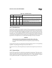
14.1.2 EPROM Devices
On EPROM devices, the quartz window must be covered with an opaque label when the device
is in operation. This is not so much to protect the EPROM array from inadvertent erasure, as to
protect the RAM and other on-chip logic. Allowing light to impinge on the silicon die during
device operation may cause a logical malfunction.
14.2 PROGRAMMING AND VERIFYING MODES
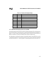
Table 14-1 lists the programming and verifying modes and provides details about the setup. The
value applied to port 0 determines the mode. The upper digit specifies program or verify and the
lower digit selects what memory function is programmed (e.g., on-chip code memory, encryption
array, configuration bytes, etc.). The addresses applied to port 1 and port 3 address locations in
the selected memory function. The encryption array, lock bits, and signature bytes reside in non-
volatile memory outside the memory address space. Configuration bytes (UCONFIG0 and
UCONFIG1) reside in nonvolatile memory at top of the memory address space for ROM/OT-
PROM/EPROM devices (Figure 4-1 on page 4-2) and in external memory for devices without
ROM/OTPROM/EPROM (Figure 4-2 on page 4-3).
14.3 GENERAL SETUP
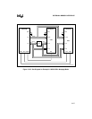
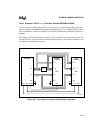
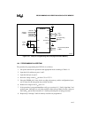
Figure 14-1 shows the general setup for programming and verifying nonvolatile memory on the
87C251Sx. The figure also applies to verifying the 83C251Sx and reading the configuration bytes
on the 80C251SB, and the 80C251SQ.
The controller must be running with an oscillator frequency of 4 MHz to 6 MHz. To program, set
up the controller as shown in Table 14-1 with the mode of operation (program/verify and memory
area) specified on port 0, the address with respect to the starting address of the memory area ap-
plied to ports 1 and 3, and the data on port 2. Apply a logic high to the RST pin and V
CC
to
EA#/V
PP
. ALE/PSEN#, normally an output pin, must be held low externally.
To perform the write operation, raise V
PP
to 12.75 V and pulse the PROG# pin per Table 14-1.
Then return V
PP
to 5 V. Verification is performed in a similar manner but without increasing V
PP
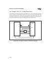
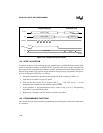
and without pulsing PROG#. Figure 14-2 shows the program and verify bus cycle waveforms.
For waveform timing information, refer to the 8XC251SA, SB, SP, SQ High-Performance
CHMOS Microcontroller Datasheet.
CAUTION
The V
PP
source must be well regulated and free of glitches. The voltage on the
V
PP
pin must not exceed the specified maximum, even under transient
conditions. See the current data sheet.


