4-11
DEVICE CONFIGURATION
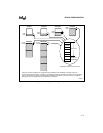
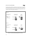
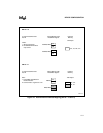
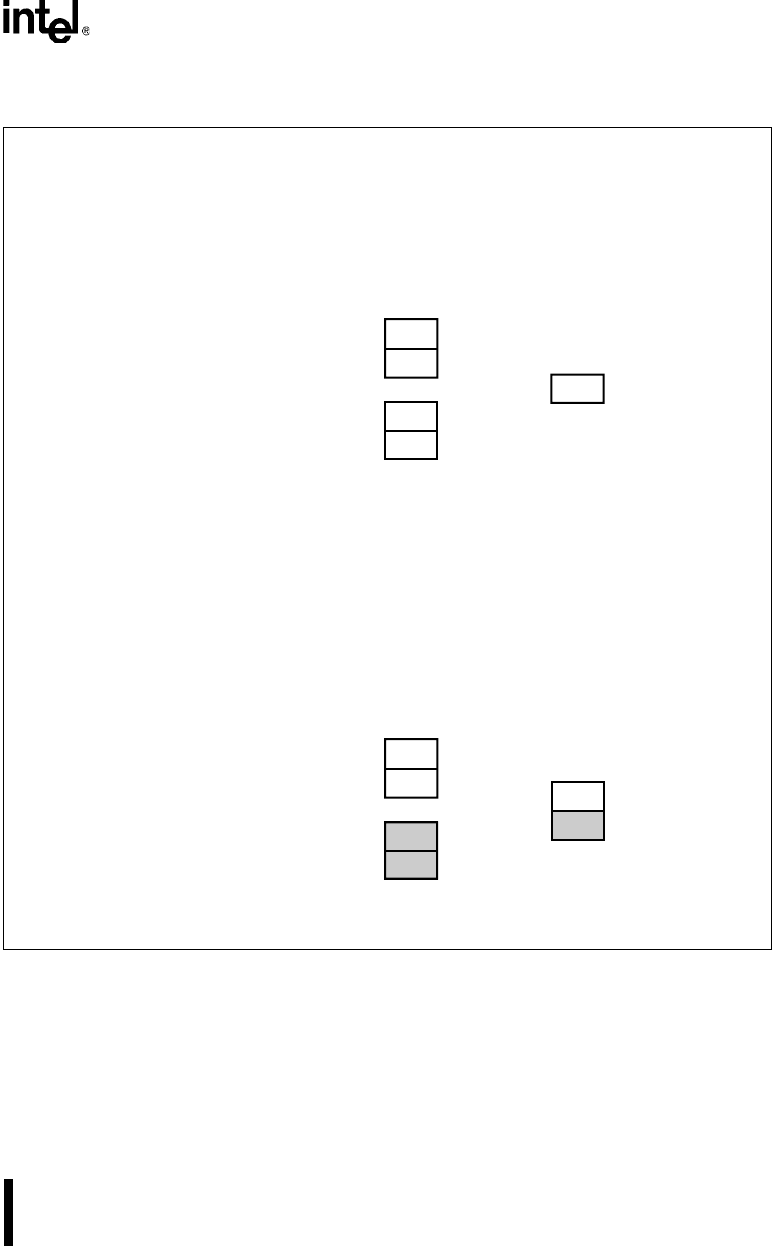
Figure 4-6. Internal/External Address Mapping (RD1:0 = 10 and 11)
FF:
01:
PSEN#
RD#, WR#
A4217-02
FF:
FE:
01:
00:
RD1:0 = 10
16 external address bits:
P0, P2
PSEN#, WR#
PSEN#, WR#
FE:, FF:
00:, 01:
00:, 01:, FE:, FF:
64 Kbytes
128 Kbytes
Notes:
1. Single read signal
2. P3.7/RD#/A16 functions
only as P3.7
Note:
1. Compatible with MCS
®
51
microcontrollers
2. Cannot write to regions FC:–FF:
Internal Memory with
Read/Write Signals
External
Memory
RD1:0 = 11
Internal Memory with
Read/Write Signals
External
Memory
16 external address bits:
P0, P2
FE:
00:


