11-5
MINIMUM HARDWARE SETUP
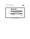
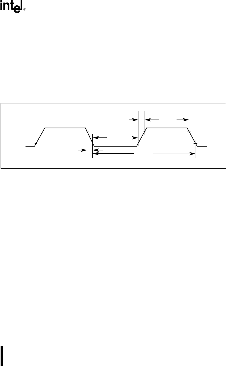
For external clock drive requirements, see the device data sheet. Figure 11-4 shows the clock
drive waveform. The external clock source must meet the minimum high and low times (T
CHCX
and T
CLCX
) and the maximum rise and fall times (T
CLCH
and T
CHCL
) to minimize the effect of ex-
ternal noise on the clock generator circuit. Long rise and fall times increase the chance that ex-
ternal noise will affect the clock circuitry and cause unreliable operation.
The external clock driver may encounter increased capacitance loading at XTAL1 due to the
interaction between the internal amplifier and its feedback capacitance (i.e., the Miller effect) at
power-on. Once the input waveform requirements are met, the input capacitance remains under
20 pF.
Figure 11-4. External Clock Drive Waveforms
11.4 RESET
A device reset initializes the 8XC251Sx and vectors the CPU to address FF:0000H. A reset is re-
quired after applying power at turn-on. A reset is a means of exiting the idle and powerdown
modes or recovering from software malfunctions.
To achieve a valid reset, V
CC
must be within its normal operating range (see device data sheet)
and the reset signal must be maintained for 64 clock cycles (64T
OSC
) after the oscillator has sta-
bilized.
Device reset is initiated in two ways:
• externally, by asserting the RST pin
• internally, if the hardware WDT or the PCA WDT expires
0.7 V
CC
A4119-01
0.45 V
V
CC
– 0.5
0.2 V
CC
– 0.1
T
CHCL
T
CLCX
T
CLCL
T
CLCH
T
CHCX


