2-5
ARCHITECTURAL OVERVIEW
2.2.1 CPU
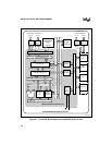
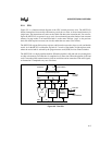
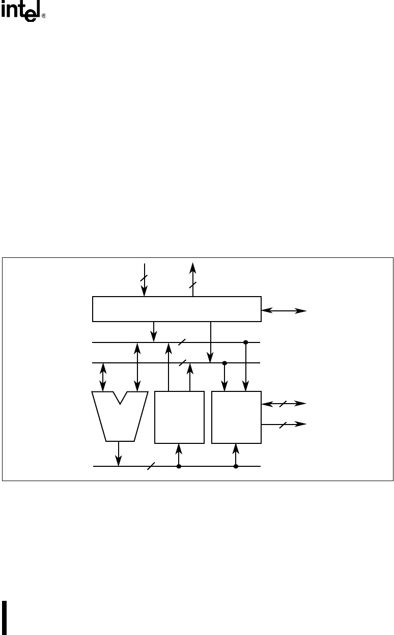
Figure 2-2 is a functional block diagram of the CPU (central processor unit). The 8XC251Sx
fetches instructions from on-chip code memory two bytes at a time, or from external memory in
single bytes. The instructions are sent over the 16-bit code bus to the execution unit. You can con-
figure the 8XC251Sx to operate in page mode for accelerated instruction fetches from external
memory. In page mode, if an instruction fetch is to the same 256-byte “page” as the previous
fetch, the fetch requires one state (two clocks) rather than two states (four clocks).
The 8XC251Sx register file has forty registers, which can be accessed as bytes, words, and double
words. As in the MCS 51 architecture, registers 0–7 consist of four banks of eight registers each,
where the active bank is selected by the program status word (PSW) for fast context switches.
The 8XC251Sx is a single-pipeline machine. When the pipeline is full and code is executing from
on-chip code memory, an instruction is completed every state time. When the pipeline is full and
code is executing from external memory (with no wait states and no extension of the ALE signal),
an instruction is completed every two state times.
Figure 2-2. The CPU
Data
Memory
Interface
Data Bus
8
16
24
Instruction Sequencer
Register
File
ALU
SRC2
SRC1
16
8
8
Code Address
Code Bus
DST
Data Address
24
Interrupt
Handler


