A-11
INSTRUCTION SET REFERENCE
A.3 INSTRUCTION SET SUMMARY
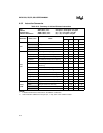
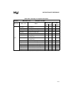
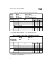
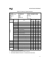
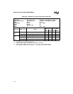
This section summarizes the MCS 251 architecture instruction set. Tables A-19 through A-27 list
the instructions by category, providing for each instruction a short description, its length in bytes,
and its execution time in states.
NOTE
The instruction execution times given in the tables are for code executing from
on-chip code memory and for data that is read from and written to on-chip
RAM. Execution times are increased by executing code from external
memory, accessing peripheral SFRs, accessing data in external memory, using
a wait state, or extending the ALE pulse.
For some instructions, accessing the port SFRs, Px, x = 0–3, increases the
execution time. These cases are noted individually in the tables.
A.3.1 Execution Times for Instructions that Access the Port SFRs
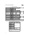
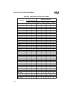
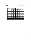
The execution times for some instructions increase when the instruction accesses a port SFR (Px,
x = 0–3) as opposed to any other SFR. Table A-18 lists these instructions and the execution times
for Case 0:
• Case 0. Code executes from on-chip ROM/OTPROM/EPROM and accesses locations in
on-chip data RAM. The port SFRs are not accessed.
In Cases 1–4, the instructions access a port SFR:
• Case 1. Code executes from on-chip ROM/OTPROM/EPROM and accesses a port SFR.
• Case 2. Code executes from external memory with no wait state and a short ALE (not
extended) and accesses a port SFR.
• Case 3. Code executes from external memory with one wait state and a short ALE (not
extended) and accesses a port SFR.
• Case 4. Code executes from external memory with one wait state and an extended ALE, and
accesses a port SFR.
The times for Cases 1 through 4 are expressed as the number of state times to add to the state
times for given for Case 0.


