10-5
SERIAL I/O PORT
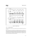
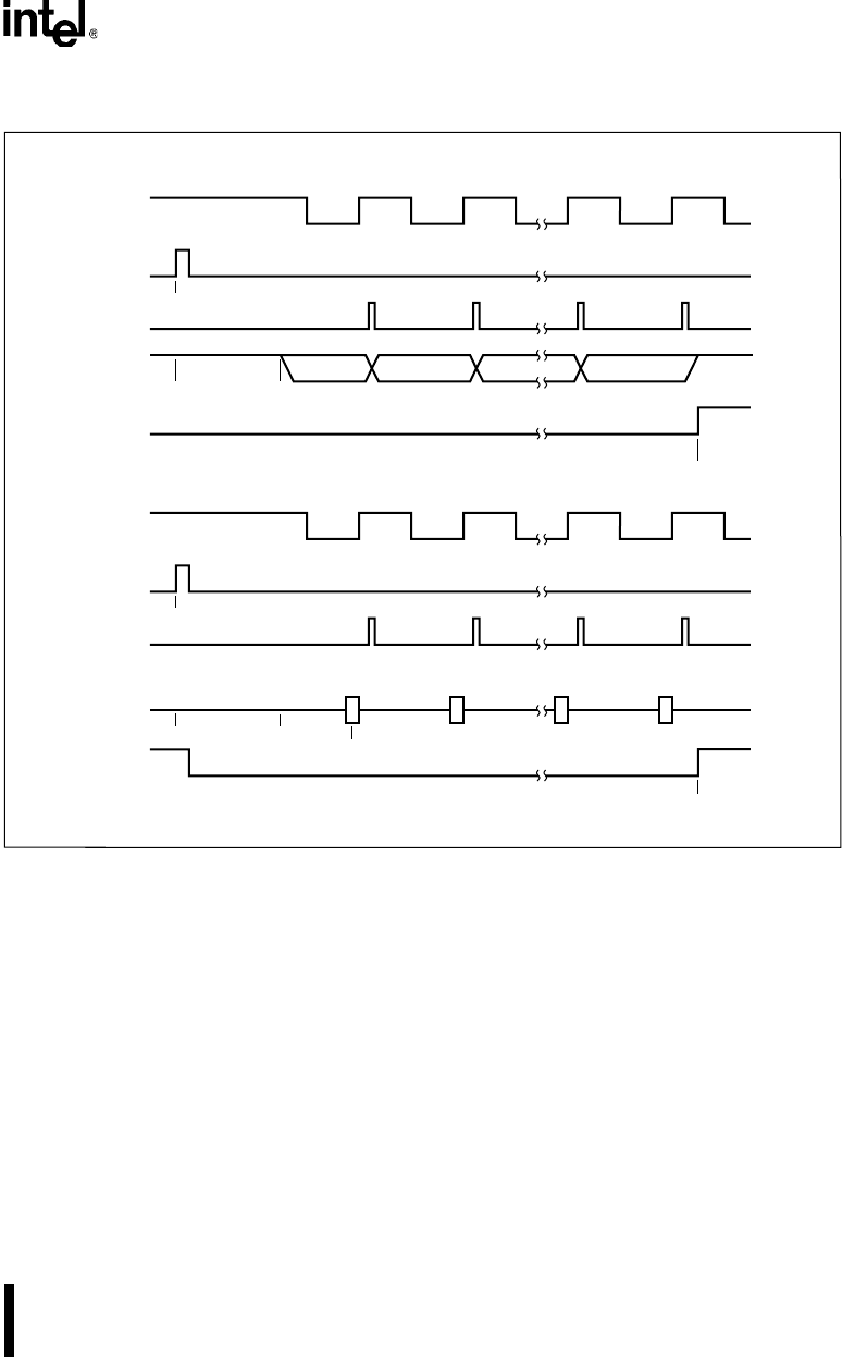
Figure 10-3. Mode 0 Timing
10.2.1.2 Reception (Mode 0)
To start a reception in mode 0, write to the SCON register. Clear bits SM0, SM1, and RI and set
the REN bit.
Hardware executes the write to SCON in the last phase (S6P2) of a peripheral cycle (Figure 10-3).
In the second peripheral cycle following the write to SCON, TXD goes low at S3P1 for the first
clock-signal pulse, and the LSB (D0) is sampled on the RXD pin at S5P2. The D0 bit is then shift-
ed into the shift register. After eight shifts at S6P2 of every peripheral cycle, the LSB (D7) is shift-
ed into the shift register, and hardware asserts RI (S1P1) to indicate a completed reception.
Software can then read the received byte from SBUF.
A4124-02
TXD
RXD
D1
Shift
S6P2 S6P2 S6P2 S6P2
Write to
SBUF
S3P1 S6P1
D2
D0
D6
D7
S6P2
S6P2
Transmit
TI
TXD
S3P1 S6P1
Write to
SCON
RI
Shift
S6P2 S6P2 S6P2 S6P2
RXD
S1P1
Receive
Set REN, Clear RI
D0
D1
D6 D7
S6P2
S5P2
S6P2
S1P1
S6P2
S6P2


