8XC251SA, SB, SP, SQ USER’S MANUAL
13-12
13.5.1 Real-time WAIT# Enable (RTWE)
The real-time WAIT# input is enabled by writing a logical ‘1’ to the WCON.0 (RTWE) bit at
S:A7H. During bus cycles, the external memory system can signal “system ready” to the micro-
controller in real time by controlling the WAIT# input signal on the port 1.6 input. Sampling of
WAIT# is coincident with the activation of RD#/PSEN# or WR# signals driven low during a bus
cycle. A ‘not-ready’ condition is recognized by the WAIT# signal held at V
IL
by the external
memory system. Use of PCA module 3 may conflict with your design. Do not use CEX3 inter-
changeably with the WAIT# signal on the port 1.3 input. Setup and hold times are illustrated in
the 8XC251SA, SB, SP, SQ High-Performance CHMOS Microcontroller Datasheet.
13.5.2 Real-time WAIT CLOCK Enable (RTWCE)
The real-time WAIT CLOCK output is driven at port 1.7 (WCLK) by writing a logical ‘1’ to the
WCON.1 (RTWCE) bit at S:A7H. When enabled, the WCLK output produces a square wave sig-
nal with a period of one-half the oscillator frequency. Use of the programmable counter array
(module 4) may conflict with your design. Do not use CEX4 interchangeably with WCLK output.
Use of address signal A17 disables both WCLK and CEX4 operation at the port 1.7 output.
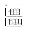
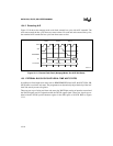
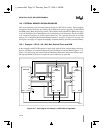
13.5.3 Real-time Wait State Bus Cycle Diagrams
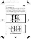
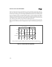
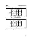
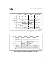
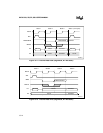
Figure 13-12 shows the code fetch/data read bus cycle in nonpage mode. Figure 13-14 depicts the
data read cycle in page mode.
CAUTION
The real-time wait function has critical external timing for code fetch. For this
reason, it is not advisable to use the real-time wait feature for code fetch in
page mode.
The data write bus cycle in nonpage mode is shown in Figure 13-13. Figure 13-15 shows the data
write bus cycle in page mode.


