8XC251SA, SB, SP, SQ USER’S MANUAL
13-8
13.3 WAIT STATES
The 8XC251SA, SB, SP, SQ provides three types of wait state solutions to external memory prob-
lems: real-time, RD#/WR#/PSEN#, and ALE wait states. The 8XC251SA, SB, SP, SQ supports
traditional real-time wait state operations for dynamic bus control. Real-time wait state opera-
tions are controlled by means of the WCON special function register. See section 13.5, “External
Bus Cycles with Real-time Wait States.”
In addition, the 8XC251SA, SB, SP, SQ device can be configured at reset to add wait states to
external bus cycles by extending the ALE or RD#/WR#/PSEN# pulses. See section 4.5.3, “Wait
State Configuration Bits.”
You can configure the chip to use multiple types of wait states. Accesses to on-chip code and data
memory always use zero wait states. The following sections demonstrate wait state usage.
13.4 EXTERNAL BUS CYCLES WITH CONFIGURABLE WAIT STATES
Three types of wait state solutions are available; real-time, RD#/WR#/PSEN#, and ALE wait
states. The 8XC251SA, SB, SP, SQ supports traditional real-time wait state operations for dy-
namic bus control. The real-time wait state operations are enabled with the WCON SFR bits at
address S:0A7H. The device can also be configured to add wait states to the external bus cycles
by extending the bus timing of the RD#/WR#/PSEN# pulses or by extending the ALE pulse or
by adding 0, 1, 2, or 3 wait states to the RD#/WR#/PSEN# pulses.
The XALE# configuration bit specifies 0 or 1 wait state for ALE. The WSA1:0# and WSB1:0#
configuration bits specify the number of wait states for RD/WR/PSEN. See section 4.5.3, “Wait
State Configuration Bits.” You can configure the chip to use multiple types of wait states. Access-
es to on-chip code and data memory always use zero wait states. The following sections describe
each solution.
13.4.1 Extending RD#/WR#/PSEN#
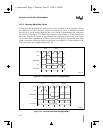
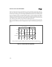
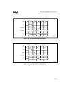
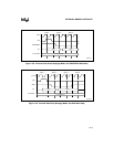
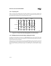
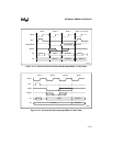
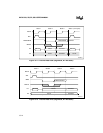
Figure 13-8 shows the nonpage mode code fetch bus cycle with one RD#/PSEN# wait state. The
wait state extends the bus cycle to three states. Figure 13-9 shows the nonpage mode data write
bus cycle with one WR# wait state. The wait state extends the bus cycle to four states. The wave-
forms in Figure 13-9 also apply to the nonpage mode data read external bus cycle if RD#/PSEN#
is substituted for WR#.


