


8XC251SA, SB, SP, SQ USER’S MANUAL
C-6
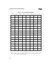
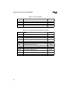
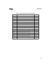
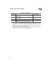
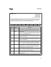
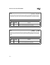
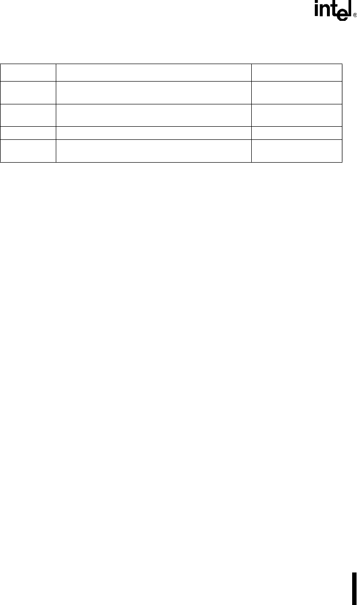
Table C-7. Register File
Mnemonic Address
R0 – R7 Four banks of 8 registers. Select bank 0-3 with bits
RS1:0 of PSW.
1, 2
R8 – R31 R11 = Accumulator (ACC)
R10 = B Register.
1, 3
R32 – R55 Reserved 3
R56 – R63 DR56 = the extended data pointer (DPXL, DPH, DPL).
DR60 = the extended stack pointer (SPH, SPL).
1, 3
NOTE:
1. The registers in the register file are normally accessed by mnemonic. Depending on its loca-
tion, a register can be addressed as a byte, word, and/or dword. See Figure 3-7 on page
3-12.
2. The four banks of registers are implemented as the lowest bytes of on-chip RAM and are
always accessible via addresses 00:0000H–00:001FH.
3. Special function registers ACC, B, DPXL, DPH, DPL, SPH, and SPL are located in the regis-
ter file and can be accessed as R11, R10, DR56, and DR60).