


7-7
INPUT/OUTPUT PORTS
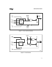
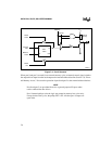
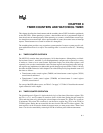
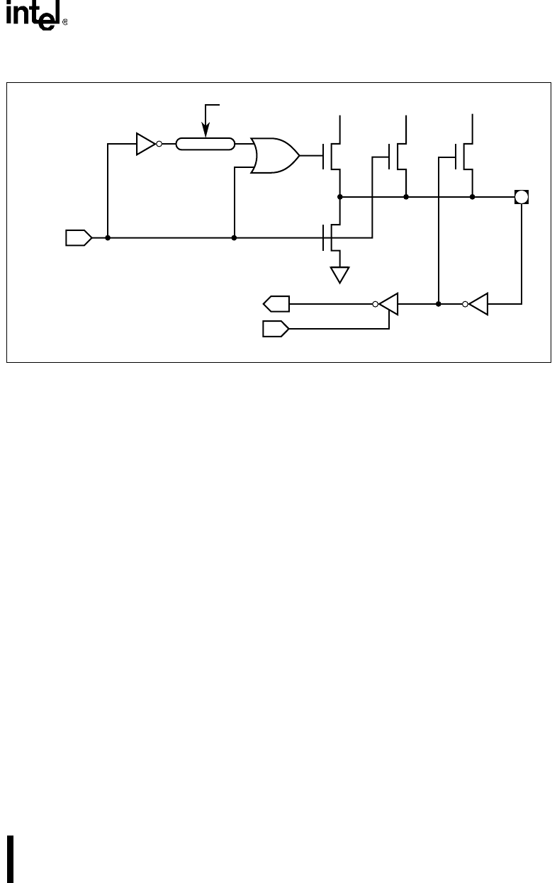
Figure 7-4. Internal Pullup Configurations
7.7 PORT LOADING
Output buffers of port 1, port 2, and port 3 can each sink 1.6 mA at logic zero (see V
OL
specifica-
tions in the 8XC251Sx data sheet). These port pins can be driven by open-collector and open-
drain devices. Logic zero-to-one transitions occur slowly as limited current pulls the pin to a log-
ic-one condition (Figure 7-4). A logic-zero input turns off pFET #3. This leaves only pFET #2
weakly in support of the transition. In external bus mode, port 0 output buffers each sink 3.2 mA
at logic zero (see V
OL1
in the 8XC251Sx data sheet). However, the port 0 pins require external
pullups to drive external gate inputs. See the latest revision of the 8XC251Sx datasheet for com-
plete electrical design information. External circuits must be designed to limit current require-
ments to these conditions.
7.8 EXTERNAL MEMORY ACCESS
The external bus structure is different for page mode and nonpage mode. In nonpage mode (used
by MCS 51 microcontrollers), port 2 outputs the upper address byte; the lower address byte and
the data are multiplexed on port 0. In page mode, the upper address byte and the data are multi-
plexed on port 2, while port 0 outputs the lower address byte.
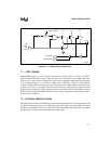
Q#
From
Port
Latch
P3
P2P1
n
Port
Input Data
Read Port Pin
2 Osc. Periods
A2242-01
V
CC
V
CC
V
CC