


8XC251SA, SB, SP, SQ USER’S MANUAL
7-6
7.6 QUASI-BIDIRECTIONAL PORT OPERATION
Port 1, port 2, and port 3 have fixed internal pullups and are referred to as “quasi-bidirectional”
ports. When configured as an input, the pin impedance appears as logic one and sources current
(see the 8XC251Sx datasheet) in response to an external logic-zero condition. Port 0 is a “true
bidirectional” pin. The pin floats when configured as input. Resets write logical one to all port
latches. If logical zero is subsequently written to a port latch, it can be returned to input conditions
by a logical one written to the latch. For additional electrical information, refer to the 8XC251SA,
SB, SP, SQ High-Performance CHMOS Microcontroller Datasheet.
NOTE
Port latch values change near the end of read-modify-write instruction cycles.
Output buffers (and therefore the pin state) update early in the instruction after
the read-modify-write instruction cycle.
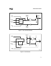
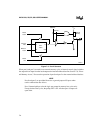
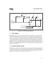
Logical zero-to-one transitions in port 1, port 2, and port 3 utilize an additional pullup to aid this
logic transition (see Figure 7-4). This increases switch speed. The extra pullup briefly sources 100
times the normal internal circuit current. The internal pullups are field-effect transistors rather
than linear resistors. Pullups consist of three p-channel FET (pFET) devices. A pFET is on when
the gate senses logical zero and off when the gate senses logical one. pFET #1 is turned on for
two oscillator periods immediately after a zero-to-one transition in the port latch. A logic one at
the port pin turns on pFET #3 (a weak pullup) through the inverter. This inverter and pFET pair
form a latch to drive logic one. pFET #2 is a very weak pullup switched on whenever the associ-
ated nFET is switched off. This is the traditional CMOS switch convention. Current strengths are
1/10 that of pFET #3.