


2-3
ARCHITECTURAL OVERVIEW
2.1 8XC251SA, SB, SP, SQ ARCHITECTURE
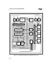
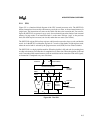
Figure 2-1 is a functional block diagram of the 8XC251SA, SB, SP, SQ. The core, which is com-
mon to all MCS 251 microcontrollers, is described in section 2.2, “MCS 251 Microcontroller
Core.” Each microcontroller type in the family has its own on-chip peripherals, I/O ports, external
system bus, size of on-chip RAM, and type and size of on-chip program memory. Table 2-1 lists
the distinguishing features of the product.
The 8XC251Sx peripherals include a dedicated watchdog timer, a timer/counter unit, a program-
mable counter array (PCA), and a serial I/O unit. The 8XC251Sx has four 8-bit I/O ports, P0–P3.
Each port pin can be individually programmed as a general I/O signal or as a special-function sig-
nal that supports the external bus or one of the on-chip peripherals. Ports P0 and P2 comprise a
16-line external bus, which transmits a 16-bit address multiplexed with 8 data bits. (You can also
configure the 8XC251Sx to have a 17-bit or an 18-bit external address bus. See section 4.5, “Con-
figuring the External Memory Interface.” Ports P1 and P3 carry bus-control and peripheral sig-
nals.
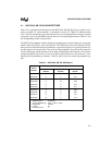
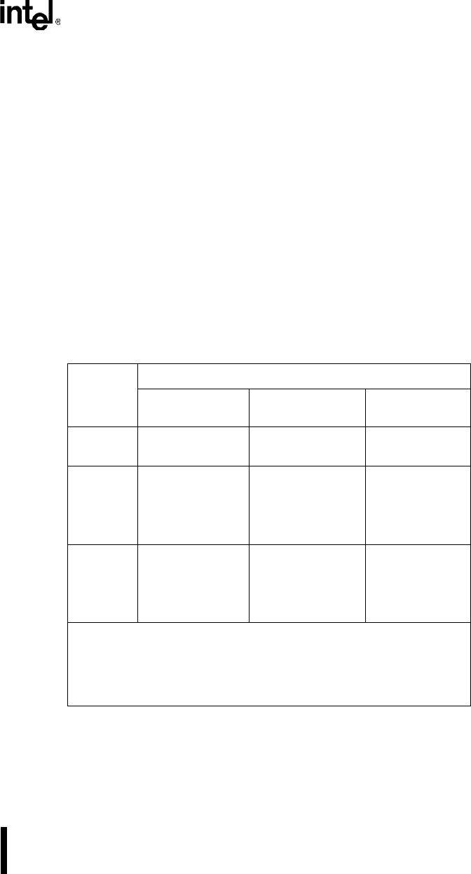
Table 2-1. 8XC251SA, SB, SP, SQ Features
Device
Number
On-chip Memory
OTPROM/EPROM
(Kbytes)
ROM
(Kbytes)
RAM
(Bytes)
80C251SB 0 0 1024
80C251SQ 0 0 512
83C251SA 0 8 1024
83C251SB 0 16 1024
83C251SP 0 8 512
83C251SQ 0 16 512
87C251SA 8 0 1024
87C251SB 16 0 1024
87C251SP 8 0 512
87C251SQ 16 0 512
Common features:
Address space 512 Kbytes
External Address bus 16-bit, 17-bit, or 18-bit
Register file 40 bytes
I/O lines 32
Interrupt sources 11