


8XC251SA, SB, SP, SQ USER’S MANUAL
7-2
7.2 I/O CONFIGURATIONS
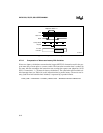
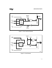
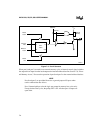
Each port SFR operates via type-D latches, as illustrated in Figure 7-1 for ports 1 and 3. A CPU
“write to latch” signal initiates transfer of internal bus data into the type-D latch. A CPU “read
latch” signal transfers the latched Q output onto the internal bus. Similarly, a “read pin” signal
transfers the logical level of the port pin. Some port data instructions activate the “read latch” sig-
nal while others activate the “read pin” signal. Latch instructions are referred to as read-modify-
write instructions (see section 7.5, “Read-Modify-Write Instructions”). Each I/O line may be in-
dependently programmed as input or output.
7.3 PORT 1 AND PORT 3
Figure 7-1 shows the structure of ports 1 and 3, which have internal pullups. An external source
can pull the pin low. Each port pin can be configured either for general-purpose I/O or for its al-
ternate input or output function (Table 7-1).
To use a pin for general-purpose output, set or clear the corresponding bit in the Px register (x =
1, 3). To use a pin for general-purpose input, set the bit in the Px register. This turns off the output
driver FET.
To configure a pin for its alternate function, set the bit in the Px register. When the latch is set, the
“alternate output function” signal controls the output level (Figure 7-1). The operation of ports 1
and 3 is discussed further in section 7.6, “Quasi-bidirectional Port Operation.”
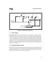
7.4 PORT 0 AND PORT 2
Ports 0 and 2 are used for general-purpose I/O or as the external address/data bus. Port 0, shown
in Figure 7-2, differs from the other ports in not having internal pullups. Figure 7-3 shows the
structure of port 2. An external source can pull a port 2 pin low.
To use a pin for general-purpose output, set or clear the corresponding bit in the Px register (x =
0, 2). To use a pin for general-purpose input set the bit in the Px register to turn off the output
driver FET.