


8XC251SA, SB, SP, SQ USER’S MANUAL
B-6
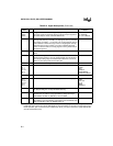
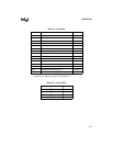
V
SS2
GND Secondary Ground 2. This ground is provided to reduce ground
bounce and improve power supply bypassing. Connection of this
pin to ground is recommended. However, when using the
8XC251SB as a pin-for-pin replacement for the 8XC51FX, V
SS2
can
be unconnected without loss of compatibility. (Not available on
DIP.)
—
WAIT# I Real-time Wait State Input. The real-time WAIT# input is enabled
by writing a logical ‘1’ to the WCON.0 (RTWE) bit at S:A7H. During
bus cycles, the external memory system can signal ‘system ready’
to the microcontroller in real time by controlling the WAIT# input
signal on the port 1.6 input.
P1.6/CEX3
WCLK O Wait Clock Output. The real-time WCLK output is driven at port
1.7 (WCLK) by writing a logical ‘1’ to the WCON.1 (RTWCE) bit at
S:A7H. When enabled, the WCLK output produces a square wave
signal with a period of one-half the oscillator frequency.
P1.7/CEX4/A17
WR# O Write. Write signal output to external memory. Asserted for the
memory address range specified by configuration byte UCONFIG0,
bits RD1:0 (Table B-3). Also see RD#.
P3.6
XTAL1 I Input to the On-chip, Inverting, Oscillator Amplifier. To use the
internal oscillator, a crystal/resonator circuit is connected to this pin.
If an external oscillator is used, its output is connected to this pin.
XTAL1 is the clock source for internal timing.
—
XTAL2 O Output of the On-chip, Inverting, Oscillator Amplifier. To use
the internal oscillator, a crystal/resonator circuit is connected to this
pin. If an external oscillator is used, leave XTAL2 unconnected.
—
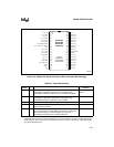
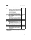
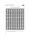
Table B-2. Signal Descriptions (Continued)
Signal
Name
Type Description
Alternate
Function
†
The descriptions of A15:8/P2.7:0 and AD7:0/P0.7:0 are for the nonpage mode chip configuration (com-
patible with 44-pin PLCC and 40-pin DIP MCS
®
51 microcontrollers). If the chip is configured for page
mode operation, port 0 carries the lower address bits (A7:0), and port 2 carries the upper address bits
(A15:8) and the data (D7:0).