


8XC251SA, SB, SP, SQ USER’S MANUAL
A-98
Example: Eight-bit register Rm contains 055H (01010101B) and the 16-bit register WRj contains
0FFFFH (11111111 11111111B). The instruction
MOVS WRj,Rm
moves the contents of register Rm (01010101B) to register WRj (i.e., WRj contains
00000000 01010101B).
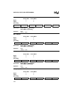
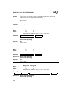
Variations
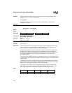
MOVS WRj,Rm
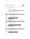
Binary Mode Source Mode
Bytes: 32
States: 21
Hex Code in: Binary Mode = [A5][Encoding]
Source Mode = [Encoding]
Operation: MOVS
(WRj).7–0 ← (Rm).7–0
(WRj).15–8 ← MSB
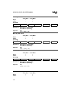
MOVX <dest>,<src>
Function: Move external
Description: Transfers data between the accumulator and a byte in external data RAM. There are two
types of instructions. One provides an 8-bit indirect address to external data RAM; the
second provides a 16-bit indirect address to external data RAM.
In the first type of MOVX instruction, the contents of R0 or R1 in the current register bank
provides an 8-bit address on port 0. Eight bits are sufficient for external I/O expansion
decoding or for a relatively small RAM array. For larger arrays, any port pins can be used to
output higher address bits. These pins would be controlled by an output instruction
preceding the MOVX.
In the second type of MOVX instruction, the data pointer generates a 16-bit address. Port 2
outputs the upper eight address bits (from DPH) while port 0 outputs the lower eight address
bits (from DPL).
For both types of moves in nonpage mode, the data is multiplexed with the lower address
bits on port 0. In page mode, the data is multiplexed with the contents of P2 on port 2 (8-bit
address) or with the upper address bits on port 2 (16-bit address).
It is possible in some situations to mix the two MOVX types. A large RAM array with its
upper address lines driven by P2 can be addressed via the data pointer, or with code to
output upper address bits to P2 followed by a MOVX instruction using R0 or R1.
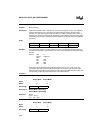
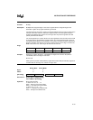
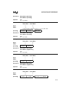
Flags:
[Encoding] 0 0 0 1 1 0 1 0 t t t t s s s s
CY AC OV N Z
—————