


7-9
INPUT/OUTPUT PORTS
NOTE
Avoid MOV P0 instructions for external memory accesses. These instructions
can corrupt input code bytes at port 0.
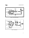
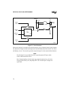
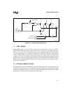
External signal ALE (address latch enable) facilitates external address latch capture. The address
byte is valid after the ALE pin drives V
OL
. For write cycles, valid data is written to port 0 just prior
to the write (WR#) pin asserting V
OL
. Data remains valid until WR# is undriven. For read cycles,
data returned from external memory must appear at port 0 before the read (RD#) pin is undriven
(refer to the 8XC251Sx datasheet for exact specifications). Wait states, by definition, affect bus-
timing.
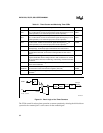
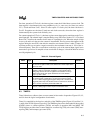
Table 7-2. Instructions for External Data Moves
Bus Width Instructions
8 MOVX @Ri; MOV @Rm; MOV dir8
16 MOVX @DPTR; MOV @WRj; MOV @WRj+dis; MOV dir16
17 MOV @DRk; MOV @DRk+dis
18 MOV @DRk; MOV @DRk+dis