


B-1
APPENDIX B
SIGNAL DESCRIPTIONS
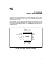
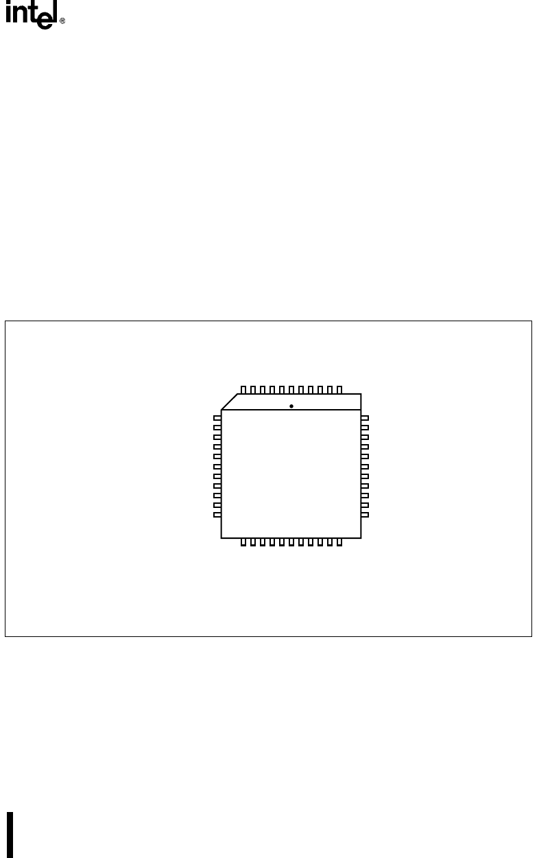
This appendix provides reference information for the external signals of the 8XC251Sx. pin as-
signments are shown in Figures B-1 (PLCC package) and B-2 (DIP package) and are listed by
functional category in Table B-1.
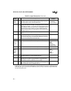
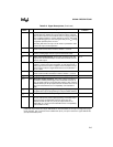
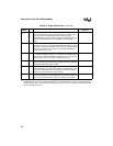
Table B-2 describes each of the signals. It lists the signal type (input, output, power, or ground)
and the alternative functions of multifunction pins. Table B-3 shows how configuration bits
RD1:0 (referred to in Table B-2) configure the A17, A16. RD#, WR# and PSEN# pins for exter-
nal memory accesses.
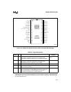
Figure B-1. 8XC251SA, SB, SP, SQ 44-pin PLCC Package
AD4 / P0.4
AD5 / P0.5
AD6 / P0.6
AD7 / P0.7
EA# / V
PP
V
SS2
ALE / PROG#
PSEN#
A15 / P2.7
A14 / P2.6
A13 / P2.5
P1.4 / CEX1
P1.3 / CEX0
P1.2 / ECI
P1.1 / T2EX
P1.0 / T2
V
SS1
V
CC
AD0 / P0.0
AD1 / P0.1
AD2 / P0.2
AD3 / P0.3
A4205-02
P1.5 / CEX2
P1.6 / CEX3 / WAIT#
P1.7 / CEX4 / A17 / WCLK
RST
P3.0 / RXD
V
CC2
P3.1 / TXD
P3.2 / INT0#
P3.3 / INT1#
P3.4 / T0
P3.5 / T1
39
38
37
36
35
34
33
32
31
30
29
8XC251SA
8XC251SB
8XC251SP
8XC251SQ
View of component as
mounted on PC board
7
8
9
10
11
12
13
14
15
16
17
P3.6 / WR#
P3.7 / RD# / A16
XTAL2
XTAL1
V
SS
V
SS2
A8 / P2.0
A9 / P2.1
A10 / P2.2
A11 / P2.3
A12 / P2.4
18
19
20
21
22
23
24
25
26
27
28
6
5
4
3
2
1
44
43
42
41
40