


8XC251SA, SB, SP, SQ USER’S MANUAL
13-20
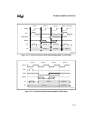
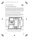
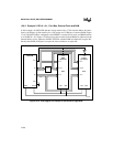
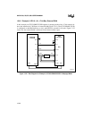
13.8.2 Example 2: RD1:0 = 01, 17-bit Bus, External Flash and RAM
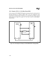
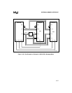
In this example, an 80C251SB operates in page mode with a 17-bit external address bus inter-
faced to 64 Kbytes of flash memory for code storage and 32 Kbytes of external RAM (Figure
13-19). The 80C251SB is configured so that PSEN# is asserted for all reads, and RD# functions
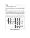
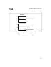
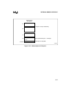
as A16 (RD1:0 = 01). Figure 13-20 shows how the external flash and RAM are addressed in the
internal address space. Addresses 0420H–7FFFH in external RAM are addressed in region 00:.
On-chip data RAM (1056 bytes) occupies the lowest addresses in region 00:.
Figure 13-19. Bus Diagram for Example 2: 80C251SB in Page Mode
PSEN#
80C251SB
A4148-01
WR#
RAM
(32 Kbytes)
OE#
FLASH
(64 Kbytes)
OE#
WE#
WE#
CE# CE#
A15:8/D7:0
A15:8
P2
P0
EA#
D7:0
A15:8
A7:0
A15:8
A7;0
D7:0
A16
A7:0
Latch
Data
Code