


8XC251SA, SB, SP, SQ USER’S MANUAL
10-4
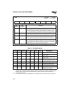
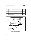
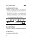
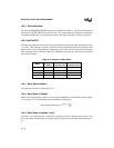
Figure 10-2. SCON: Serial Port Control Register (Continued)
10.2 MODES OF OPERATION
The serial I/O port can operate in one synchronous and three asynchronous modes.
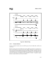
10.2.1 Synchronous Mode (Mode 0)
Mode 0 is a half-duplex, synchronous mode, which is commonly used to expand the I/O capabil-
ities of a device with shift registers. The transmit data (TXD) pin outputs a set of eight clock puls-
es while the receive data (RXD) pin transmits or receives a byte of data. The eight data bits are
transmitted and received least-significant bit (LSB) first. Shifts occur in the last phase (S6P2) of
every peripheral cycle, which corresponds to a baud rate of F
OSC
/12. Figure 10-3 shows the timing
for transmission and reception in mode 0.
10.2.1.1 Transmission (Mode 0)
Follow these steps to begin a transmission:
1. Write to the SCON register, clearing bits SM0, SM1, and REN.
2. Write the byte to be transmitted to the SBUF register. This write starts the transmission.
Hardware executes the write to SBUF in the last phase (S6P2) of a peripheral cycle. At S6P2 of
the following cycle, hardware shifts the LSB (D0) onto the RXD pin. At S3P1 of the next cycle,
the TXD pin goes low for the first clock-signal pulse. Shifts continue every peripheral cycle. In
the ninth cycle after the write to SBUF, the MSB (D7) is on the RXD pin. At the beginning of the
tenth cycle, hardware drives the RXD pin high and asserts TI (S1P1) to indicate the end of the
transmission.
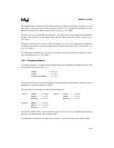
1 TI Transmit Interrupt Flag Bit:
Set by the transmitter after the last data bit is transmitted. Cleared by
software.
0 RI Receive Interrupt Flag Bit:
Set by the receiver after the last data bit of a frame has been received.
Cleared by software.