14-7
PROGRAMMING AND VERIFYING NONVOLATILE MEMORY
14.6.1 On-chip Code Memory
On-chip code memory is located in the top region of the memory space starting at address
FF:0000H. At reset, the 87C251Sx and 83C251Sx devices vector to this address. See Chapter 3,
“Address Spaces,” for detailed information on the 8XC251Sx address space.
To enter user program code and data in the on-chip code memory, perform the procedure de-
scribed in 14.4, “Programming Algorithm,” using the program on-chip code memory mode (Ta-
ble 14-1).
To verify that the on-chip code memory is correctly programmed, perform the procedure de-
scribed in section 14.5, “Verify Algorithm,” using the verify on-chip code memory mode (Table
14-1).
14.6.2 Configuration Bytes
The 87C251Sx and 83C251Sx store configuration information in an eight-byte configuration ar-
ray at FF:FFF8H–FF:FFFFH. UCONFIG0 (FF:FFF8H) and UCONFIG1 (FF:FFF9H) are imple-
mented; the remaining bytes are reserved for future use. See Figure 4-1 on page 4-2, Figure 4-3
on page 4-6, and Figure 4-4 on page 4-7.
To program the 87C251Sx configuration bytes, perform the procedure described in 14.4, “Pro-
gramming Algorithm,” using the program configuration byte mode (Table 14-1).
To verify the 87C251Sx, 83C251Sx, or 80C251SB, SQ configuration bytes, perform the proce-
dure described in 14.5, “Verify Algorithm,” using the verify configuration byte mode (Table
14-1).
14.6.3 Lock Bit System
The 87C251Sx provides a three-level lock system for protecting user program code stored in the
on-chip code memory from unauthorized access. On the 83C251Sx, only LB1 protection is avail-
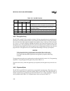
able. Table 14-2 describes the levels of protection.
To program the lock bits, perform the procedure described in 14.4, “Programming Algorithm,”
using the program lock bits mode (Table 14-1).
To verify that the lock bits are correctly programmed, perform the procedure described in 14.5,
“Verify Algorithm,” using the verify lock bits mode (Table 14-1).


